Jiwei Network reported that the establishment of the UCIe Alliance has once again made Chiplet a hot topic. With the endorsement of the head players in the semiconductor industry chain, Chiplet is expected to rewrite the technology trend and business development model of the industry in the future.
Advanced packaging is an important part of chiplet implementation, determining the ultimate success or failure of chips, but the limelight of this technology seems to be preempted by fabs. So, in the tide of Chiplet standards, what role are independent packaging companies playing, and what kind of attitude should the continental packaging industry take to meet the arrival of the standardization era?
Advanced package strength is Chiplet strong

The Chiplet concept did not come out of thin air, originating from the multi-chip module born in the 1970s, that is, a large chip composed of multiple smaller chips such as homogeneous or heterogeneous. When progress in the single-chip process slowed, Chiplet took on the responsibility of balancing chip functionality and production costs.
Before Chiplet became popular, a similar technology had become popular, and that was SiP (System in Package). SiP is defined as a plurality of active electronic devices with different functions and passive devices, as well as such as MEMS or optics, etc. assembled together to achieve a single standard package of certain functions, thereby forming a system or subsystem.
This explanation is very similar to Chiplet, both of which use packaging technology for chip combinations, what is the difference?
Shi Lei, president of Tongfu Microelectronics, believes that Chiplet can be regarded as a kind of SiP on the basis of a generalized package, because the scope of SiP is very wide, and multi-die, die and passive device combinations are all SiP. "The Chiplet mentioned now emphasizes the design of oversized dies into multiple medium/large size dies, and then wafer fabrication and packaging processing, which is considered from the perspective of subdivision. The usually mentioned SiP, the most typical is the modules in the mobile phone, its main feature is to package a large number of small size (and different functions) of small die and a large number of passive devices, mainly to emphasize the high integration of modules. Shi Lei told JiWei Network.
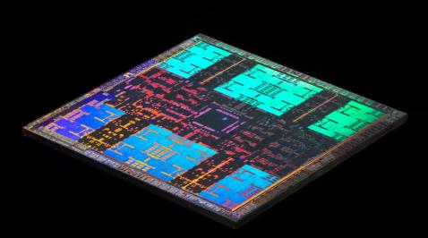
A typical Chiplet is AMD's Zen2 architecture processor, whose CPU core is manufactured separately from the I/O core, the CPU uses TSMC's 7nm process, and the I/O is GF's 14/12nm process, and the two are finally packaged into a single chip.
The difference between the two is also seen. Yu Daquan, chairman of Yuntian Semiconductor, believes that Chiplet focuses on splitting and combining, "The functional units of the chip are separated, and then re-integrated into a fully functional chip, which is equivalent to an object being dismantled into many building blocks, and then building a new thing." ”
"It can be assumed that SiP covers a large part of Chiplet, but there is a part that is not considered." Yu Daquan emphasized.
At the packaging level, Chiplet still has many similarities with SiP, using a lot of advanced packaging technology. Correspondingly, encapsulation-level challenges follow.
In Shi Lei's view, although Chiplet avoids the ultra-large die, it also means that the oversized package is highly integrated with the wafer back-channel process, and it has brought extreme technical challenges in the packaging Micro-bump, multi-layerer fan-out FO, ultra-multi-chip FC, etc., such as further increasing the accuracy and difficulty of packaging processing, further narrowing the process window, reducing the proportion of general equipment, and large demand for equipment upgrades.
Yu Daquan also believes that the technical challenge will increase, "putting different chips on the silicon interposer (intermediate layer) is the main choice of the current high-performance Chiplet, but how to connect the high-speed interface of the chip together requires a specific protocol, a micro-bump manufacturing technology, a chip stacking technology, and a TSV manufacturing technology, which is very challenging to implement." ”
Yu Daquan said: "There is also a kind of generalized Chiplet, such as putting the CPU and memory together, which can be done with TSV (silicon vias) or Fan out (fan-out package), but the accuracy requirements for wiring are very high, such as TSV's wiring accuracy is below 1μm, Fan out's wiring technology is about 2μm, which is the key packaging problem that Chiplet needs to solve." ”
The last challenge is high reliability, "because there are more chips in chiplets, more connected points, more interfaces, and the reliability problem is very serious." Yu Daquan pointed out in particular.
In addition to this, heat dissipation and power distribution are also huge issues to consider, Chiplet is going to move forward, and advanced packaging technology has a lot of challenges to solve.
Packaging plants: Opportunities and challenges coexist
The UCIe Alliance has designated a variety of advanced packaging technologies for Chiplet, including Intel EMIB, TSMC CoWoS, Sun Moon FoCoS-B, and more. It also reflects the reality that competition around advanced packaging is intensifying.
The 2021 Advanced Packaging Industry Status Report released by research institute Yole pointed out that although OSAT dominates the advanced packaging market, OSAT accounts for about 70% of the entire market in terms of primary wafers. However, in the field of high-end packaging, including 2.5D/3D stacking, high-density fan-out, large foundries (such as TSMC) and IDM (such as Intel and Samsung) are developing rapidly in the high-end market and occupying a dominant position in the market.
In recent years, TSMC has become a leader in packaging technology innovation, from CoWoS to InFO to SoIC, and has joined hands with Apple and AMD to create a number of star products, and Intel has also used self-developed advanced packaging technology in many products. For a time, the front-end packaging technology has unlimited scenery. Therefore, many people will naturally question the gradual marginalization of OSAT (outsourced test foundry) in Chiplet packaging.
Package manufacturers do not agree with this view. Shi Lei believes: "Chiplet integrates some of the fab and back-end technology, so the fab represented by TSMC has launched a packaging solution, but most of chiplet is still based on traditional and advanced packaging, and the experience accumulation and manufacturing processing of the packaging plant are also particularly important." At the same time, wafer processing focuses on universality and unity, while packaging focuses on customer individual needs, can flexibly develop various types of packaging technology expertise, and quickly provide Chiplet products that meet market demand. ”
Changdian Technology told Jiwei Network, "We have seen that in the past two or three years, front-end manufacturing and back-channel manufacturing, including design, are actively participating in heterogeneous integration, 2.5D, 3D packaging such a joint front." This reflects the inevitable trend of industrial synergy. When the front road manufacturing is in the back and the back road manufacturing is also going forward, it is inevitable that there will be common areas in the middle. But the general direction is undoubtedly that the front road manufacturing to do the front road manufacturing is good at things, the back road manufacturing to do the back road manufacturing is good at things, and finally the chiplet into the final chip finished product, which is definitely still up to the final finished product of the enterprise to do this thing. ”
"After Chiplet becomes a Chip, it also has to do packaging, whether it is Fan Out or BGA, so companies like TSMC will also find packaging plants to cooperate, because they can't package so many chips, which gives packaging plants a lot of opportunities." Yu Daquan also holds a similar view.
According to an industry insider, if the new fabs release production capacity in recent years, there will be a large number of processed wafers flowing to the back channel packaging plant, so the backway advanced packaging market still has a lot of room for improvement.
At the same time, in order to compete with fabs, package factories are also developing their own advanced packaging technologies, such as fan-out packaging technology. Although the names vary, the major packaging factories already have their own fan-out packaging technology (see the article "Micro Consulting: Fan-out Packaging is Becoming Ubiquitous").
Shi Lei believes that both board-level and wafer-level fan-out packages are the weapon for package factories to participate in Chiplet, and the world's top OSAT Chiplet technology development work has done well. Moreover, chip design companies and package factories are currently working closely together to vigorously develop Chiplet packaging.
Changdian Technology also said that the company has carried out wafer packaging technology nearly 20 years ago, and overseas factories were the first to invest heavily in fan-out wafer-level packaging technology with TSMC at that time, and carried out a large number of patents and technology development. So, it is true that this is a trend for the future development of the industry.
However, Yu Daquan also pointed out that the advantages of packaging factories in advanced packaging are not obvious, because more and more Chiplets are through holes or interconnects on active chips, and the risk of being handed over to the packaging plant will be too high.
In general, OSAT faces competition from front-line companies in the field of advanced packaging technology, and must seek to compete in a differentiated manner corresponding to low-cost high-performance packaging technology in order to continue to develop in the fierce competition.
Continental Packaging: Achieving a win-win situation on Chiplet
The packaging industry in the continental region has occupied a very important position in the world, how is chiplet packaging performing?
"There is still a gap between the mainland Chiplet packaging technology and the top manufacturers in the industry, but it is not very large. Fan-out FOMCM and multi-chip FCMCM have reached a high level, and 2.5D/3D technologies based on silicon interposer and silicon bridges are also developing. Shi Lei said.
It should be noted that the top international enterprises are packaging Chiplet on the basis of advanced processes, and wafer manufacturing in mainland China is still on the way to catch up with advanced processes.
"This does not mean that we do not have a chance, if we can implement Chiplet on the 28nm platform is also a good thing, there is no need for 14nm, 7nm process, but it also needs to have relevant companies to promote this thing." Yu Daquan thinks.
However, for the establishment of the UCIe Alliance, manufacturers still give a positive evaluation. Changdian Technology said that Chiplet still needs to form a de facto standardized process to avoid the waste of resources and technology in the process of the relatively small market size, and UCIe is a very good direction.
Shi Lei said, "The establishment time of the UCIe Technology Alliance is still relatively short, we see that there is also OSAT in the alliance, optimistic that it can promote the benign development of the Chiplet ecosystem, and can play a positive role in the development of OSAT packaging technology." ”
Jiwei Network also learned from the interview that the establishment of the UCIe Alliance is a major event in the global semiconductor industry, and the mainland industry chain is also actively participating in it. Changdian Technology said that the UCIe Alliance has a process of gradually opening up to participate in the membership, and everyone will see that other domestic manufacturers, including Changdian Technology, are actively participating in the formulation of standards. In addition, several different standardization work, including UCIe, has also been involved by domestic manufacturers.
Changdian Technology also hopes that the industry will remain patient with this standard, "The small chip itself is still just starting out, and the standardization work is a very long process, and we must look at chiplet-related standardization work with the perspective of development." This standardization should be performed by an OSAT or encapsulation process with appropriate technical capabilities. ”
Shi Lei also pointed out that in view of the complexity and difficulty of UCIe/Chiplets technology, the top enterprises in all aspects of the industry have set up alliances to discuss and solve some problems, so each link must not develop UCIe independently and blindly, and should hold an open, inclusive and win-win attitude! ”
Finally, Yu Daquan believes that the entire Chiplet industry chain needs to be strengthened, "Chiplet actually integrates a lot of technologies, including design, manufacturing, packaging, etc., so the entire industry chain must develop forward, so as to finally achieve its own Chiplet." (Proofreading/Andrew)