Source: Semiconductor Industry Watch (ID: icbank)
According to foreign media semiconductor-digest, a series of interesting events have occurred in the past few months, starting with the announcement at the Intel acceleration event in July that Amazon will be one of the first customers of Intel Foundry Services (IFS), especially in terms of packaging.
From November 30 to December 3, Amazon held their AWS re:Invent meetup, where they launched the Graviton3 data center processor. Unlike earlier Graviton and Graviton2 devices, the Graviton3 uses a small chip route with 7 dies and a total of 55 billion transistors.
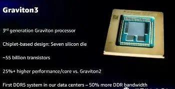
The chip on the side of the core processor chip is the DDR5 memory controller, and the bottom is the PCI-Express 5.0 controller chip. It is said to use TSMC's 5nm process, which operates at 2.6GHz and consumes 100W, which is slightly lower than the 110W of the Graviton2. There appear to be 50 billion transistors in the processor chip.
The processor has 64 cores stitched together with a mesh running at >2 GHz with a bandwidth of more than 2 TB/s. The 32 MB cache memory is distributed across the grid, and together with the core cache, the cache on the chip increases to 100 MB. The DDR controller is the DDR4800 and provides more than 300 GB/s of memory bandwidth.

Given the appearance of the Graviton3 package and the Amazon/Intel IFS package statement, I doubt that these chiplets are associated with Intel's EMIB (Embedded Multichip Interconnect Bridge) technology. Two plus two can get 22, but in Intel's last quarterly conference call, we had comments that they have shipped their first IFS package units to earn revenue since March. Graviton3 parts are now available for previewing new Amazon EC2 C7g instances, so they obviously exist in aws servers.
For me, the last confirmation link is the interconnect bump spacing reportedly 55 m; this is what EMIB uses.
So, two plus two can still get 22, but in my opinion, graviton3 at least has the possibility of using EMIB to connect these small chips together, and AWS is IFS's first revenue customer.
Intel EMIB package in-depth interpretation
The development of low-cost, heterogeneous multi-chip packaging (MCP) has driven significant system-level product innovation, leading to the emergence of three types of MCP products:
Wafer-level fan-out redistribution, using a molded plastic reconfigured wafer substrate as a surface for interconnection between dies (2D)
A separate silicon-based interconnect layer for redistribution can be a full-size silicon interposer embedded in an organic package (2.5D) or a die-to-die silicon bridge
Vertically stacked face-to-face or back-to-back chips utilizing hybrid bonding and straight-through holes from chip pads (3D)
2.5D solutions have received significant investment in R&D to support larger package sizes and greater interconnect redistribution densities (i.e., line + spacing, number of metal layers). The integration of multiple smaller dies provides a trade-off between yield and cost for chip and package assembly.
The features integrated in 2.5D MCP have become increasingly diverse, e.g., CPUs, GPUs, memory (especially HBM stacks), FPGAs, network switches, I/O transceivers, hardware accelerators for specific applications. Current R&D efforts will continue to expand the breadth of this system-in-package composition. The next "big thing" is likely to be the integration of photoelectric conversion elements to enable short- and medium-range photon-based data transmission efficiency channels.
A key aspect supporting the growth of 2.5D MCP products is the internal connection technology between dies in the package. As mentioned above, an alternative approach is to manufacture wires on a silicon intermediation layer whose dimensions are equal to the size of the entire package. Recent developments have resulted in interposers with more than 1 times the die placement and interconnection capabilities of the maximum reticle size. Another approach is to fabricate small silicon bridges for wires that span the edges of adjacent des and are embedded in organic packages.
Intel's Embedded Multi-Die Interconnect Bridge (EMIB) is an example of 2.5D MCP bridge interconnect technology. This has been briefly described in a previous SemiWiki article.
With the recent reintroduction of Intel Foundry Services, I think the technology should be studied in more depth, as it will undoubtedly become a fundamental part of the implementation of the ICF customer system.
In the most enlightening discussion with Ravi Mahajan, an Intel researcher in the Packaging and Test Technology Development Division, I had the opportunity to learn more about emib capabilities and potential. This article summarizes the main points of our discussion.
Manufacture of EMIBs
The figure above shows the cross-section of a typical EMIIB bridge designed in an organic package. The bridging silicon is located in the encapsulation cavity and is made as shown in the figure below. The top encapsulated metal layer provides a reference plane with a through hole through that plane for connecting the die and bridge.
"The EMIB process is built on a standard package construction process with additional steps to create an EMIB cavity," Ravi said. The bridge is located in the cavity and is fixed in place with an adhesive. A final dielectric layer and metal deposition layer are added, followed by through-hole drilling and plating. ”
Note that in the cross-sectional view above, the thick holes and thin holes correspond to the spacing of the two different bumps present on each die, respectively, as shown below.
Thick bumps are used for die-to-package trace layer connections, while thin spacing is associated with EMIB connections – more information about target EMIB connection density in the short term.
Ravi added: "A great deal of engineering has been carried out to define fine and rough bump profiles that will support die attachment and processing through connections. Specifically, this includes focusing on bump height control and solder volume. We've worked with bumping vendors to implement this dual pitch and profile configuration. In addition, each die in the MCP package is connected separately – the bumps on the die will be subjected to multiple reflow cycles. Note the flux material that binds to the bump. Methods have also been developed to provide a void-free epoxy resin underfill agent throughout the bump area. Materials, bumps and attachment processes are all carried out in mass production. ”
EMIB physical implementation
An example of a bridge-only is shown below. This specific design implements the following features:
The pitch of the bumps to the die is 55um
2um line + 2um spacing, metal thickness of 2um
4um spacing, 250 wires per millimeter "beachfront"
The dielectric thickness between each EMIB metal layer is 2um
The 4 metal layers M1 and M3 on the EMIB bridge are dedicated to the GND plane
Typically on M2 and M4 a signal layer of 3 signal + 1 ground shield pattern is utilized
To be precise, as shown in the figure below, the metal planes on the standby EMIB layer are implemented as meshes.
"The design of EMIB interconnects is a complex trade-off between multiple targets – interconnect density (number of wires per millimeter edge, bumps per millimeter**2), power limits, and signal bandwidth," Ravi said. For each die, this means driver size and receiver sensitivity. To save power, unterminated receivers are often used (i.e., capacitive load only, resistor-free termination). To address these goals, EMIB design considerations include line and space size, bump spacing, channel length, metal thickness, and dielectric material between metal layers. The design of electrical signal shielding (e.g. S1G1, S2G1, S3G1) is also crucial. ”
The figure below shows a layout diagram of the interconnect density design, including how the bridge signal reaches the multi-line fine-pitched bumps on adjacent die. The following table describes the range of available sizes and spacing.
The following illustration shows the various bridge positioning options. Note that the placement of bridges has a great deal of flexibility - for example, horizontally and vertically, in an asymmetrical position relative to the edge of the mold.
EMIB electrical characteristics
Intel has published a detailed electrical analysis of the EMIB interconnect, evaluating insertion loss and crosstalk for various signal ground shield combinations and wire lengths.
The image above highlights the power distribution paths in the package. Note that the EMIB bridge has a small footprint, which means that the balance of I/O signal and power integrity characteristics is not affected, unlike the all-silicon mediation layer, where all signal and power vias must first pass through the mediation layer. As mentioned earlier, the top package layer above the EMIB is also used as a ground plane.
The following figure shows an example of the results of the electrical analysis, depicting the maximum EMIB signal length of the target accumulated beach front bandwidth for various signal shielding modes. In this example, a radical L/S line spacing design is employed. Electrical model used:
A simple output driver (R = 50ohms, C = 0.5pF)
Unterminated receiver (C = 0.5pF)
Four-layer EMIB metal stack, dielectric constant = 4.0
The top encapsulation metal plane above the recessed bridge
EMIB Design Services
Due to the complexity of the EMIB design trade-offs, Ravi said: "Intel will work closely with foundry customers on product requirements and develop EMIB design as a service. Together with our customers, we will work with customers on die lead lines and bump patterns and provide EMIB silicon implementations that meet their data rate targets. ”
Future development of EMIB
EMIB technology remains Intel's research and development focus. Ravi emphasizes: "We will continue to work on providing greater interconnect edge density, including tighter bump spacing and more aggressive line/space EMIB metal spacing (less than 1um)." Integrating active circuitry into EMIB is certainly also feasible. ”
summary
The EMIB bridging approach that supports advanced MCP technologies has some unique advantages:
Expansion of existing organic packaging technology
Supports large chip count and large package configurations
Lower cost than full-size silicon interlayers
Use simple driver/receiver circuitry to support high data rate signaling between adjacent chips
Optimize the capability of each die-dice link individually by customizing the bridge for the link
EMIB links feature high efficiency, low metal R*C latency, minimal latency, and high signal integrity.
Intel's R&D team has addressed some of the drawbacks of EMIB:
Additional complexity in the chip bump and package assembly process
The coefficient of thermal expansion (CTE) between the package, die, and EMIB bridges is different
EMIB silicon thins (t.) before package assembly
The support provided by Intel Foundry Services' packaging team will help customers seeking advanced MCP solutions achieve their signaling data rate, power, and cost goals.
There is no doubt that the growth in MCP package adoption will continue to accelerate. (The DARPA CHIPS program will also generate greater interest in MCP design.) )
What do you think about this? Comments are welcome
---- the full text ends here, if you like, please click "Watching" or share to the circle of friends.
- END -