This article is reproduced from [Semiconductor Industry Observation Public Number]
Back in 1965, computer scientist Gordon Moore hypothesized that the number of transistors and other components integrated in the chip would double approximately every two years, while doubling the speed and capacity of computers. But after 55 years, the number of transistors that can be stuffed into a single chip is almost at its limit.
However, the road ahead for computing systems has not slowed down. Dynamic AI systems are ready to power every aspect of our lives – from road safety to drug discovery and advanced manufacturing – which will require more powerful chips in the future. For the chip industry to continue to move forward at moore-assumed speed and computing power, we need to make chips with up to 100 billion transistors.
In order to achieve this goal, manufacturers in the industry are exploring a variety of solutions. IBM Research is also deeply involved, announcing that the company has made a breakthrough in semiconductor design cooperation with Samsung. With a type called the Vertical-Transport Nanosheet Field Effect Transistor (VTFET), Moore's Law can continue to work for years to come.
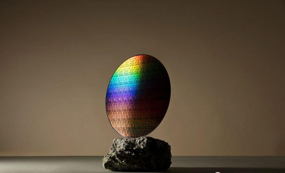
VTFET (Vertical Transmission Nanosheet Field Effect Transistor) wafers
VTFET: Make 1nm possible
According to IBMji, today's major chip architectures are transverse transmission field-effect transistors (FETs), such as fin-type field-effect transistors or FinFETs (named because the silicon body resembles the dorsal fin of a fish), which layers the transistors along the surface of the wafer. VTFETs, on the other hand, place the transistor perpendicular to the silicon policeman and direct the current perpendicular to the surface of the silicon wafer. This new approach addresses scaling barriers by breaking down physical limitations on transistor gate length, spacer thickness, and contact size in order to optimize various parameters including performance and power consumption.
With VTFETs, IBM successfully demonstrated that it is possible to explore scaling beyond nanosheet technology in CMOS semiconductor designs. On these advanced nodes, VTFETs deliver twice the performance boost or up to 85% power savings compared to the scaled FinFET alternative. 1
The new VTFET architecture demonstrates a way to perpetuate Moore's Law beyond nanosheets. In May of this year, Google announced a 2-nanometer node chip design that will enable the chip to install up to 50 billion transistors in a space the size of a fingernail. VTFETs continue their journey of innovation, opening the door to new possibilities.
In the past, designers packaged more transistors onto the chip by reducing the gate spacing and routing spacing. The physical space that fits all components is called contact gate pitch (CGP). The ability to reduce the gate and routing spacing has enabled integrated circuit designers to increase transistors from thousands to millions to billions in our devices. However, for state-of-the-art FinFET technology, space, gates, and contacts have limited space. That means that once you reach your CGP limit, you don't have room to continue to shrink.

Fet configuration on the silicon horizontally. Virtual isolation gates shown in blue are required to isolate adjacent circuits that waste space.
With vertically directional current, gates, spacing, and contacts are no longer limited by traditional methods: we have room to expand the CGP while maintaining healthy transistor, contact, and isolation (isolation and shallow trench isolation, STI: spacer and shallow trench isolation) dimensions. Freed from the limitations of lateral layout and current flow, we were able to use larger source/drain contacts to increase the current on the device. The gate length can be selected to optimize the device drive current and leakage, while the isolation layer thickness can be independently optimized to reduce capacitance. We are no longer forced to make trade-offs between gate, spacer, and contact size, which can increase switching speed and reduce power consumption.
The new VFET configuration arranges layers vertically on the wafer, significantly improving density scaling by reducing the barrier spacing and eliminating the virtual isolation barrier.
Another key VTFET feature is the ability to use STI for adjacent circuit isolation to achieve zero diffusion interrupt (ZDB: Zero-Diffusion Break) isolation without losing active gate spacing. In contrast, the density of a transverse transmission FET circuit is affected by the double or single diffusion interrupts required for circuit isolation, which affects the ability to further shrink the technology.
A decade ago, we could see that lateral architectures would reach scaling limits at aggressive gate spacing: virtually every component of the device was close to the scaling limit. We wanted to find other ways to break down these barriers, and our motivations never changed. Our goal has always been to produce competitive equipment for the technology of the future.
Because the gate spacing is more aggressive than any product known in production, and cmOS logic transistors with a gate spacing of less than 45 nm on the body silicon, we believe that the VTFET design represents a huge leap forward in building the next generation of transistors that will enable smaller, more powerful, and more energy-efficient devices in the coming years.
GAA: 2nm transistor selection
As mentioned earlier, IBM has announced how the company will achieve 2nm in May this year, so let's take a closer look at IBM's implementation method.
According to IBM, their new Gate-All-Around (GAA) nanosheet architecture enables it to integrate 50 billion transistors in a space the size of a fingernail. This paved the way for the realization of the 2 nanometer (nm) node.
However, IBM also stressed that their demonstration of the nanosheet transistor at the 2nm chip node is also a validation of several smaller milestones that have shown us that this approach is feasible and that the collaboration of IBM's interdisciplinary team of experts in materials, lithography, integration, equipment in the project, characterization and modeling is complementary.
A row of 2 nm nanosheet devices observed using transmission electron microscopy. 2 nm is smaller than the width of a single strand of human DNA
IBM further noted that since they first proposed the name "Nanosheet" in the summer of 2012 to describe the new device architecture they were working on at the time, the company's consistent idea had been to develop a flake structure rather than the nanowire structure we've been using. In their view, the newly named nanosheet architecture will be able to provide electrostatic advantages that nanowires do not have, while also having the density needed to improve performance. IBM emphasizes that only through the combination of these features can IBM Research provide a transistor architecture that is superior to FinFETs.
IBM also said that the second iteration of the company's nanosheet transistor architecture involved a new type of horizontally stacked GAA chip design. The four "gates" on the transistor enable excellent electrical signals to pass through and between other transistors on the chip.
2 nm transistor of nanosheet structure
IBM further emphasized that another milestone for the company's 2nm is 2017. Because in the same year they officially introduced the nanosheet transistor, they also realized that the inner spacer module in the transistor architecture would be a key enabler of the nanosheet's performance, which could be achieved by reducing the capacitance from the gate to the source/drain. IBM says Inner spacers are key structural components because they define the effective gate length of a GAA device. In 2019, the team worked with partner companies to develop a new inner spacer process using dry indent techniques. This allows for process control of less than 1 nm as well as improved inner spacer profiles.
By combining this new dry inner spacer isolation process with the industry's first bottom dielectric isolation, IBM was able to create a gate length of 12 nanometers that is only two dozen atoms long. The benefit of a full bottom dielectric isolation scheme is that it reduces sub-channel leakage, provides immunity to process variations, and provides power performance improvements.
Notably, recent advances in transistor size — such as 10 nm, 7 nm, 5 nm, and now 2 nm nodes — refer to specific generations of chips manufactured using specific types of semiconductor manufacturing processes, much like 5G refers to the latest wireless standards. In this case, for example, 2 nm does not correspond to half the spacing of the traditionally defined contact metal wire. In general, smaller technology nodes produce smaller transistors, where more transistors can be packaged onto the chip, making them faster and more energy efficient.
In May, IBM researchers also used extreme ultraviolet (EUV) lithography for the first time to develop nanosheet devices with a width of 15 to 70 nm at the front end (FEOL), demonstrating that the technology can produce smaller lines than visible light. FEOL is the first part of integrated circuit fabrication, in which transistors and other components form patterns in semiconductors. IBM said it was the first research institute to discuss introducing EUV to FEOL. IBM Research's Albany Lab has one of the most advanced EUV lithography tools in the industry. It allows for more precise control of nanosheet width and greatly simplifies the process of putting low-power and high-performance designs on the same chip.
Another key highlight in the company's first 2 nm transistor, according to IBMjIE, is the development of a new multi-threshold voltage (Multi-Vt) device with leakage levels spanning three orders of magnitude. This allows device manufacturers to better select the level of performance required by the underlying chip architecture.
IBM says phones with 2nm processors can improve battery life by a factor of four compared to phones that use 7nm processor technology, such as the iPhone 11, Samsung Galaxy S10 and Google Pixel 5. Based on average usage, this means that the phone can only need to be charged once every four days.
Using the same power, a transistor scaled to a 2 nm chip node equates to approximately 45% better performance than today's 7 nm chips. At the same performance level, this can save approximately 75% of the power. This power/performance combination is critical to accelerating the development and delivery of advanced cognitive, edge, and other computing platforms delivered through hybrid cloud environments, as well as cryptographic accelerators built to run with quantum computers.
IBM Research said at the time that the company would continue to explore ways to continue to expand to 1 nm (the VTFET mentioned at the beginning) and more advanced processes. Breaking through these barriers is critical to enabling IBM to continue to deliver the hardware that enterprises rely on to adopt the latest, most advanced artificial intelligence and hybrid cloud technologies.
In IBM's view, while we are still a few years away from making 2 nm node chips, IBM Research's innovations are directly integrated into our commercial product roadmap. For example, the industry's first commercial 7 nm processor is based on IBM Research's breakthrough in 2015.
Going forward, IBM hopes to leverage its leadership in semiconductor innovation to allow cloud providers or other large data center operators to use fewer servers to do the same amount of work, reducing energy costs and carbon footprint.