◎ Science and Technology Daily reporter Hualing
Recently, professor Ren Tianling's team at the School of Integrated Circuits of Tsinghua University has made a breakthrough in the research of small-size transistors, and for the first time prepared a transistor with a sub-1 nanometer gate length, which has good electrical properties. The results were published in the latest issue of Nature online.
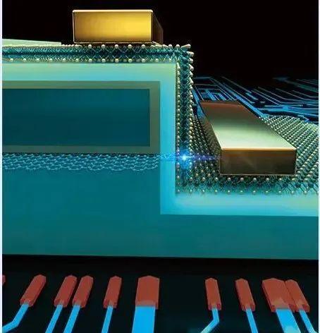
Schematic diagram of sub-1 nanometer gate-length transistor structure. Image source: Tsinghua University official website
Transistors are the core components of the chip, and the smaller gate size allows more transistors to be integrated on the chip and improve performance. Over the past few decades, the gate size of transistors has been driven by Moore's Law. However, in recent years, as the physical size of transistors has entered the nanoscale, the short-channel effects such as reduced electron mobility, increased leakage current, and increased static power consumption have become more and more serious. Therefore, the development of new structures and new materials is imminent.
At present, the gate size of transistors in mainstream industry is above 12 nanometers. In order to further break through the bottleneck of the gate length transistor below 1 nanometer, Ren Tianling's team cleverly used the ultra-thin single atomic layer thickness and excellent conductivity of the graphene film as a gate to control the switching of the vertical molybdenum disulfide (MoS2) channel through the graphene lateral electric field, so as to achieve an equivalent physical gate length of 0.34 nanometers.
"It was very difficult to break this record for quite some time." Li Huamin, a nanoelectronics scientist at the State University of New York at Buffalo, commented that the new work further narrows the size limit of the gate to "the thickness of only one layer of carbon atoms." So, for the research of small transistors, how did you think of using graphene materials to break through the bottleneck?
"The thickness of the single layer graphene is only 0.34 nanometers, so using graphene as the gate enables a very short gate size. Graphene itself is a planar structure, which requires the channel to be a vertical structure, and to achieve a vertical channel structure is one of the problems. In addition, graphene in addition to the sidewall can be gated, its surface can also be gated, so shielding the graphene surface electric field is also a difficult point, we developed a self-oxide layer to shield the graphene surface electric field. On March 20, Ren Tianling said in an interview with a reporter from Science and Technology Daily.

With the development of Moore's law, the transistor gate length was gradually reduced, and the transistor with a sub-1 nanometer gate length was realized in this work. Image source: Tsinghua University official website
How to make gate-length transistors below 1 nanometer move from laboratory results to industrialization? Ren Tianling replied: "The gate-length transistor below 1 nanometer is only a dimensional size microfilm, and in the future, it will also need to cooperate with the microcollection of the channel, which requires the help of lithography machines, such as further scaling the channel size to 5 nanometers through extreme ultraviolet (EUV) lithography, and further realizing ultra-large-scale chips." ”
If this research achieves the world's smallest gate length transistor and pushes Moore's Law further to the sub-1 nanometer level, does it mean that this is also a new beginning, and there will be new explorations - the birth of smaller transistors?
"Yes, this is indeed a new beginning, and there will be new explorations – the birth of smaller transistors." In the face of reporters' questions, Ren Tianling replied affirmatively, "The premise is that a single-layer material with a smaller atomic size can be developed." Materials that are currently smaller than carbon atoms on the periodic table are potential candidates, but it should be noted that these materials smaller than carbon atoms do not currently have a single atomic layer structure, so it is difficult to produce smaller-level transistors in the future. For example, the use of hydrogen atoms for gate control is likely to be the ultimate size of the gate length of transistors, but the preparation of metal hydrogen itself is a worldwide problem, although Science reported metal hydrogen in 2017, but the metal hydrogen pole is unstable, and there is no single atomic layer structure, so it is very difficult. ”
So, in the application of integrated circuits in the future, how will this two-dimensional film give the related products different performance?
Ren Tianling introduced: "The future integrated circuit of two-dimensional thin film will bring flexible, higher density, transparent electronic products, such as the current hot flexible electronic screen, but the current CPU is not flexible, if the use of two-dimensional materials, there is an opportunity to achieve a fully flexible mobile phone, including CPU, memory can also be soft." For this work, our team has achieved lower power transistors in addition to achieving the world's smallest gate length transistors, which means that future chips can be more energy efficient. ”
"This scientific research work belongs to the research team after a long period of accumulation to obtain a result, the intermediate process is full of challenges." This work is China's independent intellectual property rights, and in the future, we will continue to carry out trench scaling and large-scale chip integration to make a contribution to China Core. Ren Tianling stressed.
Source: Science and Technology Daily
Editor: Zhang Qiqi
Review: Julie
Final Judge: He Yi