According to the Taiwan media Lianhe Bao, TSMC's 3-nanometer process will be introduced into mass production in August this year, but TSMC decided to turn the 3-nanometer research and development team to 1.4-nanometer development in order to gain hegemony and prevent Intel from grabbing orders, and is scheduled to start shooting next month and invest in the first phase of confirming technical specifications (TV0) development, which also prepares TSMC to step into the 1-nanometer generation and open a new page in history.
The report further pointed out that TSMC recently finalized in August this year in the Bamboo Research and Development Center P8 plant and Nanke 18B P5 plant, after the start of 3-nanometer mass production at the same time in the north and south, the next step is to suppress Intel through the 2-nanometer technology to break through the threat of Apple's new generation processor, in order to continue to maintain a leading edge in wafer foundry.
Considering that both Samsung and Intel are eyeing the cake on TSMC's mouth. There is no doubt that another round of chip process competition is about to start.
TSMC was in a hurry
At the previous earnings report, Wei Zhejia, co-president of TSMC, once said that the company's 2nm process is under development, such as according to the preliminary plan, trial production will be at the end of 2024, and the fastest will be put into mass production in 2025. However, Intel had said earlier that the company would complete the chip design of intel 18A (about 1.8nm) in the second half of this year and advance the original mass production time from the previous 2025 to 2024. From this, we can see the source of TSMC's concerns.
On the other hand, readers who have an understanding of the process should know that the 3nm process that started the war in the second half of this year has been promoted to the present, in fact, the fundamentals have been determined. Because of the process schedule of the three major manufacturers (TSMC, Intel and Samsung), even customers are initially determined at present, and the possibility of too much change in the short term is relatively small.
However, in the technical node after 3nm, there is a new uncertainty.
As we all know, since Intel released the 22nm process in 2011, intel, TSMC, Samsung, GF and SMIC have used FinFET transistors on almost all advanced process logic chips. Unlike previous planar transistor channels, they are horizontal. In FinFET, the channel is vertical and the gate surrounds the channel, providing excellent control from the three sides of the channel.
Because of this unusual design, FinFETs bring more advantages in applications. For example, a given transistor footprint has a higher drive current, higher speed, and lower leakage, which enables it to have lower power consumption, no random dopant fluctuations, and allows the transistor to have better mobility and scaling. With this innovative transistor design, the chip manufacturing process evolved to the 3nm that came out in the second half of this year. Because in addition to Samsung, other wafer foundries still use FinFET at this node.
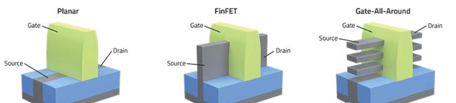
Planar transistors, FinFET transistors and GAA transistors
However, by the time of 3nm, finFET's historical mission has been completed, which has driven all wafer foundries to explore new manufacturing methods, such as the GAA (Gate All Around) transistor applied by Samsung on 3nm. Just as it did when it was originally turned from plane to stereoscopic, the new transistors will also present new challenges for developers. It should be noted that Samsung used this new transistor in 3nm, and Intel also disclosed a lot of information about their new transistors, and they regarded Intel 18A as a key technology beyond TSMC. In addition, the Nikkei News recently reported that the United States and Japan are planning to cooperate on 2nm chips. Considering Japan's leading position in equipment, the current trend of local chip manufacturing, ibm's past glorious history in advanced technology in the United States, and the boom, they also launched 2nm chips a year ago.
This makes TSMC, which is doing a very good job of secrecy in the new process, anxious.
GAA is not that simple
As mentioned above, GAA transistors are an inevitable development trend in the industry, and nanosheets are the first choice of GAA transistors.
The so-called nanosheet, from the structural point of view, the nanosheet FET is a finFET rotated 90 degrees, which allows it to produce a horizontal stack of fin, and each fin has a vertical gate material in the middle, and each fin is a channel.

Lam Research introduced in a blog post in 2020 that early GAA devices will use vertically stacked nanosheets. They consist of separate horizontal sheets surrounded by door material. This provides improved channel control over finFETs. Unlike FinFETs, where higher currents require multiple side-by-side fins, the current carrying capacity of GAA transistors is increased by vertically stacking several nanosheets, with the gate material wrapped around the channel. The size of the nanosheets can be scaled so that the size of the transistors can meet the specific properties required.
The blog post further notes that nanosheets may be conceptually simple, but they present new challenges for manufacturing. Some of these challenges revolve around the fabrication structure, while others involve the new materials needed to achieve the PPAC expansion goals.
As shown in the figure, GAA transistors are fabricated by first growing alternating Si and SiGe epitaxial layers of superlattices that form the basis of nanosheets. Key steps include depositing an internal dielectric spacer to protect the source/drain region and defining the gate width, as well as channel release etching to remove the sacrificial layer. The space left after removing the sacrificial layer needs to be filled with gate dielectrics and metals, including between the nanosheets. Because gate metals are likely to introduce new materials, some manufacturers are evaluating cobalt, ruthenium, molybdenum, nickel, and various alloys.
In semiengineering's report, they also revealed the significant challenges posed by making nanosheet FETs.
First, in the process, the epitaxial tool deposits ultra-thin, alternating Layers of SiGe and silicon on the substrate to form a superlattice structure. This structure may have three, five or more layers of each material; second, tiny vertical fins are patterned and etched in a superlattice structure. Then, an inner spacer is formed. In spaced etching, the outer part of the SiGe layer in the superlattice structure is dented and then filled with dielectric material; third, a source/drain is formed. The SiGe layer in the superlattice structure is then removed, leaving behind the silicon substrate or sheet that make up the channel; finally, the gate is formed by depositing a high k dielectric and a metal gate material.
"Each of these steps is a challenge. As with all processes, the goal is to develop chips without defects. This requires a well-developed process control strategy in the fab. Semiengineering's reporter emphasized in the article. (For nanosheet manufacturing, refer to the Semiconductor Industry Watch article "Successors to FinFETs: How Should Nanosheets Be Manufactured?") 》)
TSMC's manufacturing integration manager first emphasized in an interview with the IEEE in February this year that we are approaching the atomic scale. He then continues: "Previously, we could achieve next-generation nodes by fine-tuning processes, but now with each generation we have to find new approaches in terms of transistor architecture, materials, processes, and tools. In the past, this was almost a major optical zoom, but it was no longer a simple trick. ”
Lam Research said that GAA transistors will become the successor to FinFET, while nanosheets will evolve into nanowires. These GAA structures should cut through the high-level process nodes on the current roadmap.
The Big Three have their own tricks
It is precisely because the new technology has such a big challenge, so the three giants are working day and night to conquer the new manufacturing process, and they have also disclosed some layouts for their new technologies for the future.
First of all, let's look at the more "urgent" TSMC. At ISSCC 2021, TSMC Chairman Deyin Liu gave a speech in which he roughly introduced TSMC's nanosheet technology. Liu Noting noted that the drains of these new devices cause lower barrier reductions and smaller sub-threshold swings. According to reports, next-generation platforms using TSMC have reduced the supply voltage of SRAM, allowing it to provide reliable caching operation at 0.46V. And as the demand for on-chip caches continues to increase, voltages below half a volt will certainly improve the chip power budget.
Although TSMC did not disclose much at the seminar, according to some analysts, the data displayed by TSMC came from 32 MB of SRAM, but no other technical details were given. They ventured to guess that its M0 spacing was 28 nm, just like in the 5N process, which is that the width of the nanosheet is about 35 nm and the thickness is about 6 nm. It is this design that gives it a channel width of 240–250 nm, or a 2+ fin transistor equivalent to the current fin height.
Semiwiki said in an article that Jin Cai of TSMC's R&D group conducted a discussion called "CMOS Device Technology for the Next Decade" at last year's VLSI symposium. In his speech, he revealed three areas of TSMC's active process development, describing ways to obtain more optimized nanosheet properties: increasing the SiGe stoichiometry of pFET, optimizing parasitic Cgs/Cgd capacitors, and dealing with "mesa" leakage from bottom nanosheets. (For details, refer to the article "TSMC Talks about the Implementation of 2nm").
Next, let's take a look at Samsung, which is one step ahead. Because he brought the company's GAA transistor manufacturing process in the second half of this year, that is, the MBCFET (multi-bridge channel FET) manufacturing process used by Samsung in 3nm.
Official Samsung documents indicate that a typical GAA transistor takes the form of elongated nanowires. However, the channel needs to be as wide as possible to allow a large amount of current to flow through it, and the small diameter of the nanowires makes it difficult to obtain this higher current. To overcome this problem, Samsung created and patented their proprietary MBCFETs (Multi-Bridge Channel Field Effect Transistors). In Samsung's view, this is an optimized version of the GAA transistor. By aligning the channel structure formed by the wires into two-dimensional nanosheets to increase the area in contact with the gate, MBCFETs enable simpler device integration as well as increased current. In Samsung's view, the company's MBCFET is a competitive transistor structure because it includes not only methods to mitigate the short-channel effect through a GAA structure, but also improves performance by expanding the channel area.
Finally, take a look at Intel's GAA transistor RibbonFET
According to reports, RibbonFET devices can raise the channel from the substrate material to form a channel line into a gate material. Because the channel line is shaped like a ribbon, the new FET technology is called RibbonFET, and the gate surrounds the channel completely. This unique design significantly improves the electrostatic characteristics of transistors and reduces transistor size with the same node technology. But that's not the only technical improvement Intel has made; they've also developed a new power routing technology called PowerVia. Conventional semiconductors have planar semiconductors that form transistors and then add wire layers to provide power and signals. Mixing power and signals creates routing challenges and reduces the overall efficiency of the final device.
Intel's newly announced PowerVia can move the power connection of the transistor to the bottom of the chip. In short, the introduction of PowerVia is equivalent to the transfer of PCBs from single-sided layers to duplex layers. Allows the power and signal lines to be separated, making both layers more efficient.
summary
It can be seen from the above that whether it is TSMC, Samsung or Intel, they are actually fully prepared for GAA to welcome the arrival of the next node. At the same time, they are also continuing to develop future-oriented processes, so that the performance of chips has more options. For example, two-dimensional materials are a direction of efforts for fabs, including TSMC.
According to the researchers, two-dimensional semiconductors are expected to solve the problem of channel control in large transistors: reducing device size also reduces channel length. Interfacial defects (due to the small size of the transistor gate channel) result in decreased carrier mobility. Transition metal disulfides (TMDs) such as MoS2 are the material of choice for sub-10nm channel transistors because of their high mobility at extremely thin thicknesses.
In the middle of last year, TSMC announced that the company and the Massachusetts Institute of Technology (MIT) jointly published a study, for the first time proposed the use of "semi-metallic bismuth" (Bi) as a two-dimensional material contact electrode, which can greatly reduce the resistance and increase the current, so that its efficiency is almost the same as that of silicon, which will help achieve the challenge of 1 nanometer of semiconductors in the future.
In addition to these fab manufacturing leaders, research institutions such as IMEC are proposing many solutions and improvements for future chip implementations. The future of chip manufacturing is still promising.
Source: Content by Semiconductor Industry Watch (ID: icbank) original, author: Mu Zi, thank you.