CES is approaching, and various news about AMD's new CPU seems to have been exposed in advance.
According to foreign media reports, amD Zen4 architecture will be manufactured using TSMC's 5nm process, and the corresponding products include Ryzen™ 7000 Rapheal for desktop, Ryzen™ 7000H/7000U Pheonix for notebooks, and Xiaolong 7004 Genoa in data centers.
We've heard before that the Zen5 architecture will use a size core configuration, but it looks like Zen4 will be on the size core in advance!
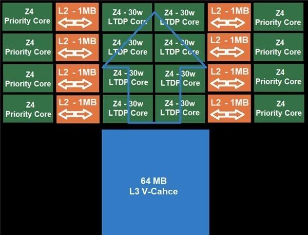
Among them, the large core is the complete Zen4, also known as the "Priority Core", each Die (CCD) has 8, the small core is the residual version (LTDP) that reduces the power consumption of the thermal design, each Die is also 8, the total thermal design power consumption is 30W, an average of 3.75W per each.
It is said that the Zen4's Ryzen™ 7000 series thermal design consumes up to 170W, so the average is 17.5W per large core.
In terms of caching, each pair of size cores shares 1MB of L3 cache, for a total of 8MB, and all cores share 64MB of L3 cache, but it does not look like it is directly integrated, but is additionally stacked in the form of v-Cache.
The upcoming Zen3 V-Cache version has a V-Cache stack cache, but it comes with a level 3 cache plus additional stacking.
Such a design, if it is a two Die (CCD) integrated package, a single processor can easily achieve 32 cores, 128MB level three cache.
In other aspects, Zen4 will also switch to the new AM5 LGA1718 package interface, support dual channel DDR5-5200 memory, 28 PCIe 5.0 channels, NVMe 4.0, USB4, with the motherboard is expected to be X670, B650.
(7844235)
![Buy is earn! AmD Zen 4 Ryzen™ 7000 processors will be extremely tight[fig]](data:image/gif;base64,R0lGODlhAQABAIAAAP///wAAACwAAAAAAQABAAACAkQBADs=)