Semiconductor authority imec recently released the latest news in the industry, the most important news is the High NA (high numerical aperture) EUV lithography machine, ASML in advance of its mass production, 0.55NA's next generation of EUV lithography machine No. 1 trial machine may be mass production in 2026.
ASML revealed that the first NA EUV lithography machine opened for early testing in 2023 and began mass production from 2025, but analysts believe this is not realistic.
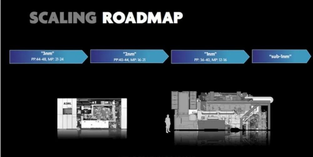
Why do you want to develop a new generation of lithography machines, before the bad? The iteration of the lithography machine has enabled this device to have higher lithography resolution, more efficient production efficiency, and a simpler lithography process. Correspondingly, the lithography machine equipment and chip process matching, at present, the most advanced chip process process is 3nm, the existing EUV lithography machine can also meet its needs, but for the next generation of 2nm process process, a little bit not enough to see, you need High NA EUV lithography machine will shoulder the heavy responsibility.

The so-called High NA EUV lithography machine, is to make the lithography machine have a higher resolution by adjusting the parameters of the lens, its working principle is basically the same as the EUV, but its special envoy lens can be magnified in two directions at the same time, one magnified by 8 times and one magnified by 4 times. This allows light to pass through the reticle at more angles, improves the resolution of the imaging pattern, and is key to solving the cost issues associated with EUV multiple patterns. With this in mind, the chip produced by this machine should be the fastest and most efficient in history.
Why not look forward to the mass production of high NA EUV lithography machine in 2025? Industry insiders say the cost of a High NA lithography machine is expected to be $316.8 million, but in fact the total cost may be higher, because the new system requires new equipment, new photomasks and different photoresists to operate. Suppliers are doing their best to develop new technologies, but there are still some gaps with their goals.
The energy use efficiency of the EUV lithography machine is not high, the transmission of EUV light requires a special mirror, each transmission will lose 30% of the energy, in the machine on average more than 10 times of reflection process, and finally less than 2% of the light energy is left. Take TSMC, the power consumption of EUV is more than 10 times that of DUV, and through the improvement of the machine and the analysis of big data, the energy use efficiency has been increased by 5%, but it is still far from enough, which has led to the development of high NA equipment. Some believe that the machine is expected to allow the chip manufacturing industry to follow Moore's Law for at least another 10 years.
In addition, the energy use efficiency of the EUV lithography machine is not high, the transmission of EUV light requires a special mirror, each transmission will lose 30% of the energy, in the machine on average more than 10 times of reflection process, and finally less than 2% of the light energy. Take TSMC, the power consumption of EUV is more than 10 times that of DUV, and through the improvement of the machine and the analysis of big data, the energy use efficiency has been increased by 5%, but it is still far from enough, which has led to the development of high NA equipment. Some believe that the machine is expected to allow the chip manufacturing industry to follow Moore's Law for at least another 10 years.
It is conceivable that there are still a few who have money to buy it, but owning it also means that it has the right to speak in the field of chip manufacturing in the future. As early as July this year, Intel expressed its commitment to becoming the first customer of high-NA lithography machines, which is related to its ambition to return to the industry boss.
In recent years, Intel has been pulled away by TSMC and Samsung in the chip manufacturing process, and even the yield rate of the 10nm process has been pulled, resulting in delayed mass production. After painful thinking, Intel's new CEO Kissinger proposed the IDM2.0 strategy, one of which is to improve the process technology of its own chips, and more advanced chip manufacturing, the need to have better, more EUV equipment, in the world's three major fabs, Intel is also currently the manufacturer who buys the least EUV tools, and the most purchased is TSMC. So Intel took aim at the EUV lithography machine.
Based on the strong capabilities of the EUV lithography machine, only fabs of 7nm or less can exert its strength, in order to meet the "entry threshold", Intel spent $20 billion to establish a factory in Arizona to ensure its chip manufacturing capabilities. Intel CEO Henry Kissinger said that the full embrace of EUV lithography machines is to make consumers more confident in them.
Layout of the latest generation of EUV lithography machine, Intel will grab the EUV lithography machine to accelerate to the white-hot stage, advanced lithography machine manufacturers only ASML, although it is expanding production, but as of now, only shipped more than 100 EUV machines, in the face of the three major fabs, ASML production has become a new bottleneck.