"This article is original, plagiarism is prohibited, and violators must be investigated"
Since the signing of the "Wanason Agreement", many US companies and other foreign semiconductor companies have been affected by technical restrictions and cannot freely ship to the mainland.
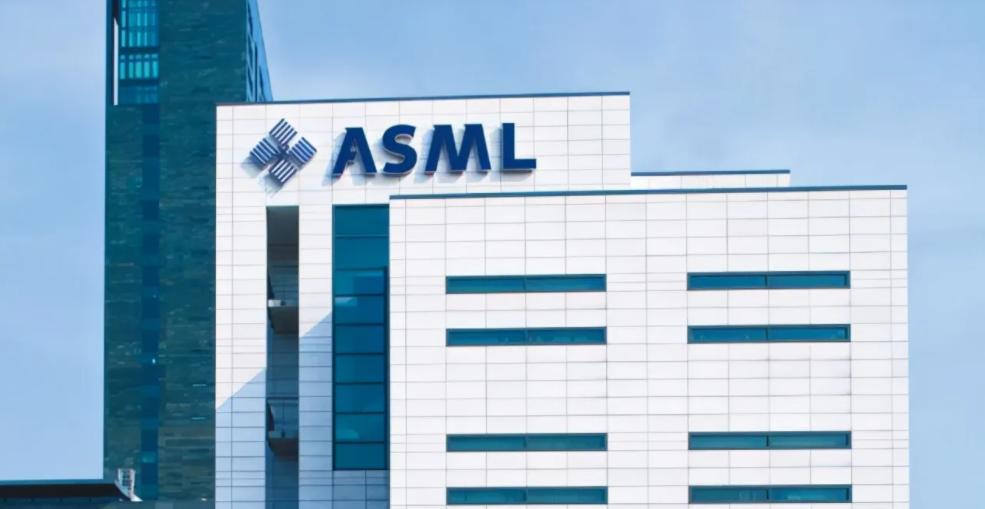
As the world's leading lithography equipment manufacturer – as well as ASML. Although ASML is a Dutch company, some of its lithography equipment manufacturing uses American technology and components, so its lithography equipment cannot be freely shipped to the mainland.
However, for the current situation of "global lack of cores", the absence of lithography machine is equivalent to the inability to increase the production capacity of chip manufacturing, especially high-process chips below 7nm, to manufacture almost no EUV lithography machine.
It is reasonable to say that the demand for lithography equipment is unprecedented, the market for ASML should be very good, and the status should also rise, but ASML has recently faintly appeared to be abandoned by the international environment.

According to the traditional chip manufacturing method, the chip should be manufactured by DUV (deep ultraviolet) lithography machine, or EUV (extreme ultraviolet) lithography machine to produce. In particular, the current manufacturing technology of EUV lithography machine is monopolized by ASML. To a certain extent, ASML almost determines the fate of many semiconductor companies.
Why did ASML, which has such a huge advantage, fall to this point? There are three main points.
Due to the revision of the "chip rules", many companies have not been able to purchase the most advanced EUV lithography equipment. This has led many companies to realize the importance of self-research of lithography equipment, and have opened up the research and development of lithography equipment and new chip manufacturing technologies.
China's self-developed lithography equipment and new packaging process
First of all, the mainland has started the research and development of lithography equipment early. Under the leadership of the Chinese Academy of Sciences, Guowang Optics and Changchun Guo research jointly issued the 28nm node ArF immersion lithography exposure system, and the key technology of the high NA immersion optical system, which marks the realization of the mainland's high-end lithography machine exposure optical system with independent intellectual property rights.
On March 23, 2022, according to the news released by the Beijing Public Resources Trading Service Platform, the Guowang Optical Lithography Machine Exposure System Production Base Project is being tendered, and there are currently three candidates for bidding.
The R&D and production base of the project is built by Beijing Guowang Optics, and the core team members of the R&D team are from Changchun Guoke Precision. The base will be used for the research and development and production of ultra-precision optical industry technology.
In the later stage, the mass production of high-end precision optical instruments and equipment will be slowly realized, and a more complete large-scale IC manufacturing projection lithography exposure optical system will be established. The problem of industrialization of the mainland's IC manufacturing projection lithography machine exposure optical system and high-end precision optical equipment has been fundamentally solved.
Shanghai Microelectronics has also developed the first 2.5D / 3D advanced encapsulated lithography machine, which was officially delivered to customers on February 7 this year.
Huawei has also developed a new chip stacking technology and applied for a corresponding chip stacking packaging equipment patent. In the future, we will take the way of exchanging area for performance, replacing Kirin chips with stacked chips to improve product competitiveness.
TSMC has developed a new 3D packaging process, and it is possible to achieve mass production of up to 5nm process.
In addition, many international enterprises have also begun to develop lithography machines and advanced processes
After the Russian chip market was "cut off", it was announced that it would develop its own lithography machine, with an initial investment of 670 million rubles (equivalent to about 51 million yuan). At present, MIET (Moscow Electronics Technical Institute) has taken over the project.
Unlike ASML's principle of EUV lithography machine, Russia is a maskless X-ray lithography machine developed based on the principle of synchrotron or plasma source.
Russia's maskless X-ray lithography machine will be used in the production of process chips from 28nm to 16nm and below.
Kai-Chi has also partnered with Canon and DNP to develop a mass-production nil (nano-embossing microscopy technology). NIL's microscopic process is relatively simple, with 10% lower power consumption than EUV production methods, less energy consumption, and equipment investment reduced to 40%.
Through NIL technology, it has been possible to achieve mass production of 15nm process, and it is expected to break through the mass production of lower processes in 2025, and the circuit fineness can reach up to 5nm.
Samsung also launched the GAA transistor process and is currently in trial production of the 3nm process.
The establishment of the Chip Alliance
In order to get rid of the dependence on ASML lithography equipment, but the self-developed EUV lithography machine is an impossible task, many companies have begun to develop new chip packaging technology.
In addition to Huawei's chip stacking and TSMC's 3D packaging process, Apple has developed the "glue bonding method", based on TSMC's 5nm process, the two MAmax chips are simply and rudely put together, encapsulating the M1 Ultra chip, even the A15, which is known as the strongest chip, can not match it, and the performance is 50% higher than the A15.
Under the leadership of TSMC and Intel, Microsoft, Qualcomm, AMD, Arm, Google Cloud, Meta, and Samsung jointly established the "Chip Alliance".
The alliance will develop a common set of standards, so that each self-developed "small chip" can achieve a higher degree of compatibility, allowing different merchants to mix and match chips, so that different small chips can be interoperable.
If there is no unified standard, each self-developed small chip does not have a unified size and performance standards, in the subsequent mass production and launch, it is difficult to adapt, the establishment of the small chip alliance also indicates the international recognition of advanced packaging technology.
conclusion
From these, it can be seen that many international companies are gradually reducing their dependence on ASML lithography machines. While not yet possible, IT is likely to be slowly abandoned by the market in the near future.
What is your opinion that ASML's lithography machine is slowly being abandoned by the market? Feel free to leave your own insights in the comments section.