(Report Producer/Author: Haitong International)
1. Silicon carbide (SiC): a new generation of semiconductor materials, opening up a market space of 10 billion yuan for new energy vehicles
1.1 Silicon carbide semiconductor materials
The third generation of semiconductors has superior performance and a wider range of application scenarios. As the foundation for the development of electronic information technology, semiconductor materials have undergone several generations of changes. With the higher requirements of application scenarios, the third generation of semiconductor materials represented by silicon carbide and gallium nitride has gradually entered the stage of industrial acceleration. Compared with the previous two generations of materials, silicon carbide has superior properties such as high pressure resistance, high temperature resistance and low loss, and is widely used in the production of high temperature, high frequency, high power and radiation-resistant electronic devices.
Silicon carbide devices have a wide range of application scenarios. Because of its high thermal conductivity, high breakdown electric field strength and high current density, semiconductor devices based on silicon carbide materials can be applied to many industrial fields such as automobiles, charging equipment, portable power supplies, communication equipment, mechanical arms, and aircraft. The scope of its application is also constantly popularizing and deepening, and it is a material with a very wide application prospect and great value.
1.2 Advantage analysis of silicon carbide
The band gap width of the third generation of semiconductor materials is much larger than that of the previous two generations. The first and second generation semiconductors are narrow bandgap semiconductors, and from the third generation of semiconductors, wide bandgap (bandgap greater than 2.2eV) semiconductor materials have begun to be widely used. As a typical representative of the third generation of semiconductors, silicon carbide has more than 200 spatial structures, and different structures correspond to different band gap values, generally between 2.4eV-3.35eV. In addition to the wide bandgap, silicon carbide material also has the advantages of high breakdown field strength, high saturation drift speed, high stability, and maximum power.
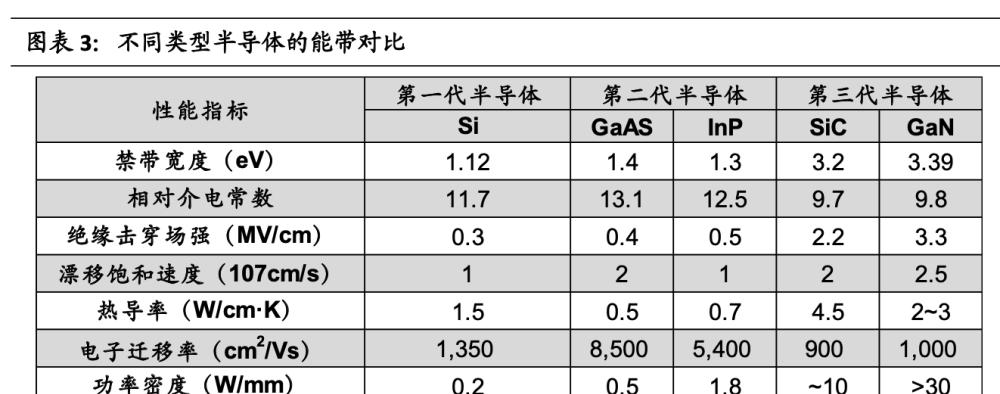
1.2.1 Wide bandgap: Improve material stability and breakdown of electric field strength
The band gap width determines the material properties, and the wide band gap improves better performance. Band gap width is an important indicator to measure the performance of semiconductors, wider band gap means higher excitation requirements, that is, electrons and holes are more difficult to form, which also leads to wide bandgap semiconductors can maintain similar insulator characteristics when they do not need to work, which also makes it have better stability, wide band gap also helps to improve the strength of the breakdown electric field, and then enhance the ability to withstand the working environment, which is embodied in better heat resistance and high voltage resistance, radiation resistance.
At the same time, due to the high energy difference between the conductive band and the valence band in the wide bandgap system, the compound rate of electrons and holes after being excited is greatly reduced, which makes more electrons and holes can be used for conduction or heat transfer, which is also a reason why silicon carbide has stronger thermal conductivity and electrical conductivity.

Based on these characteristics, silicon carbide devices can work in higher strength environments, can also dissipate heat more quickly, and have higher limit operating temperatures. The high temperature resistance can lead to a significant increase in power density while reducing the requirements on the heat dissipation system, making the terminal more lightweight and miniaturized. The high band gap width of silicon carbide also makes the leakage current of silicon carbide devices significantly reduced than that of silicon devices, thereby reducing power loss; Silicon carbide devices do not have current tailing phenomenon during the shutdown process, and the switching loss is low, which greatly increases the switching frequency of practical applications.
1.2.2 High breakdown voltage: brings a larger operating range and power range
The higher the breakdown voltage, the greater the operating range and power range. Breakdown voltage refers to the voltage at which the dielectric is broken. For semiconductors, once the voltage reaches the breakdown voltage, it means that the semiconductor loses its dielectric energy, and because the internal structure is destroyed, it exhibits a performance similar to that of a conductor, and thus cannot work. Therefore, a higher breakdown electric field means a larger operating range and power range, that is, the higher the breakdown electric field, the better.
Silicon carbide devices are more powerful, smaller and have lower energy losses. Because of its higher breakdown voltage characteristics, silicon carbide materials can be widely used in the preparation of high-power devices, which is an irreplaceable advantage of silicon-based semiconductors. Higher electrical breakdown of silicon carbide allows silicon carbide power devices to have a thinner and heavier doped barrier layer, which makes the use of silicon carbide materials under the same requirements can make the device thinner, which can play a role in saving space and improving the unit energy density. In addition, the high breakdown electric field can also make the silicon carbide in the external voltage less on resistance, and the smaller on resistance means lower energy loss.
1.2.3 High saturation drift rate: less energy loss
Silicon carbide has a higher saturation drift rate due to its internal structure. The drift velocity reflects the migration speed of the carrier under the external voltage, theoretically speaking, the drift rate can be infinitely increased with the increase of the external electric field, but in fact, with the increase of the external electric field, the collision between the carriers inside the material will also increase, so there will be a saturated drift rate. In silicon carbide materials, its internal structure has a good ability to buffer collisions, so it has a higher saturation drift rate.
The high saturation drift rate results in less energy loss. The high saturation drift rate means faster carrier migration and lower resistance. This also makes the energy loss in the silicon carbide material much reduced. Compared with silicon, the on-resistance of the same specification of the silicon carbide MOSFET and the silicon MOSFET are reduced to 1/200 and the size is reduced to 1/10; The use of siC-based MOSFETs of the same specifications results in a total energy loss of less than 1/4 compared to inverters using silicon-based IGBTs. These characteristics provide strong support for the application of silicon carbide materials in photovoltaic inverters and high-frequency devices.
2. Silicon carbide industry chain
Foreign manufacturers mostly lay out in the IDM mode, and domestic enterprises focus on a single link. The silicon carbide industry chain can be divided into: substrate, epitaxy, device, and terminal application. Foreign companies mostly lay out the whole industry chain in the IDM mode, such as Wolfspeed, Rohm and STMicroelectronics (ST), while domestic companies focus on single-link manufacturing, such as Tianke Heda and Tianyue Advanced in the substrate field, Hantian Tiancheng and Dongguan Tianyu in the epitaxial field, and Star Peninsula and Tyco Tianrun in the device field.
Substrates and epitaxy account for 70% of the cost of siC devices. Subject to the difficulty of preparation of the material end, low yield, small production capacity, the current value of the industrial chain is concentrated in the substrate and epitaxial part, the front end of the two parts accounted for 47%, 23% of the cost of silicon carbide devices, while the back-end design, manufacturing, packaging and testing links accounted for only 30%.
2.1 Substrate: The industry presents a super pattern
The industry is a super-dominant pattern, with Wolfspeed accounting for 62% of the market. Since Tesla first introduced silicon carbide devices into the Model3 instead of IGBT modules in 2018, it has opened up the application of silicon carbide in the field of new energy vehicles, and the industry has rapidly entered a warming period. At present, the silicon carbide substrate market presents a super pattern, Wolfspeed (formerly Cree).
62% of the market share is the first, II-VI, Rohm with 14% and 13% market share ranked second and third, CR3 is close to 90%. The market share of domestic manufacturers Tianke Heda is only 4%.
Silicon carbide substrates can be divided into conductive and semi-insulated types. Conductive type refers to the silicon carbide substrate with resistivity of 15~ 30mΩ·cm, which can be further made into power devices after it is extended, and is applied to new energy vehicles, photovoltaics, smart grids and other fields. The semi-insulated type refers to the silicon carbide substrate with a resistivity higher than 105mΩ·cm, which is mainly used to manufacture gallium nitride microwave RF devices as basic components in the field of wireless communication.
Silicon carbide substrate is synthesized into SiC micropowder by high-purity silicon and toner, grown into crystal ingots by physical vapor deposition (PVT), and then processed to obtain a standard diameter size silicon carbide crystal, and then obtained a silicon carbide polishing sheet with no damage on the surface through the cutting and polishing process, and finally tested and cleaned to form a silicon carbide substrate that can be delivered to downstream epitaxial manufacturers.
2.1.1 Raw material synthesis: each substrate manufacturer mainly produces itself
High-purity SiC powder can be synthesized using gas phase method, liquid phase method and solid phase method, and the current industry mainly uses the solid phase method in the self-propagating high-temperature synthesis method, that is, the solid Si source and the C source as raw materials, so that it can continue to react at a high temperature of 1400 ~ 2000 °C, and finally obtain a high-purity SiC powder. This method has cheap raw materials, stable synthesis quality and high synthesis efficiency. At present, each substrate manufacturer basically produces its own high-purity SiC powder.
2.1.2 Crystal ingot growth: At present, the PVT method is the main method in the industry, and the overall yield is low
90% of substrate companies choose the PVT method. Silicon carbide single crystal mainly has physical vapor transport method (PVT), high temperature chemical vapor deposition (HTCVD) method and liquid phase epitaxial method (LPE) method, the current PVT method is the most mature process in the industry due to the advantages of easy manufacturing of equipment, better control of long crystal process and lower cost. The principle is to be in
SiC raw materials above 2000 °C are sublimated and decomposed into gaseous substances, which are transported to the seed crystals with lower temperatures and crystallized to form SiC single crystals. 90% of the industry uses the PVT method.
The principle of the HTCVD method is to chemically react SiC to SiC in a high temperature environment of about 2100 °C, which can achieve long-term continuous crystal growth, but the equipment cost is high and the growth rate is also very slow. The HTCVD method is used by Norstel and Denso in the industry.
The LPE method precipitates silicon carbide crystals from the supersaturated liquid by dissolving the carbon in a high-temperature pure silicon solution. LPE is suitable for the preparation of high-quality large-size silicon carbide substrates, but the growth rate is extremely slow, the material requirements are also high, and the application manufacturers include Sumitomo Metals.
The PVT method has a slow growth rate, low thickness, and low yield. According to the data of Liu Dewei et al. in the article "Research on the Process of Growing 6-inch 4H-SiC Crystals by PVT Method", under the temperature of different raw material areas, the thickness of the crystal ingot is 8-15mm within 80 hours of growth time, and due to the influence of the graphitization of the powder source, the length of the crystal ingot is limited to about 50mm. And the growth environment of silicon carbide crystals is complex, the process control is difficult, the overall yield is low, according to Tianyue Advanced Prospectus, the overall yield of the company's crystal rod link is 50%.
2.1.3 Cutting and grinding: SiC crystal ingot has high hardness, high brittleness, and difficulty in processing
After the growth of the finished SiC ingot is initially processed and finalized, it also needs to be cut and polished to make a silicon carbide polishing sheet. Restricted by processing technology, the current processing efficiency of high surface quality silicon carbide wafers is low, according to Tianyue Advanced Prospectus, the overall yield of the company's substrate link is 75%.
The domestic cutting link is mainly multi-line cutting with consolidated abrasives. Due to the high hardness, brittleness and chemical stability of silicon carbide, traditional sawing tools cannot be used. At present, the most used consolidation abrasive multi-wire cutting method in China is used to process, and the diamond abrasive is consolidated on the metal wire, and the sawing process of abrasive particles is realized with the movement of the saw wire. At present, laser cutting, cold separation and EDM slicing technologies are being studied at home and abroad.
Grinding is mainly to remove defects in the surface after the chip is cut and achieve a predetermined thickness, while minimizing the warping, bending, total thickness change, and surface roughness of the wafer. At present, single-sided thinning technology and double-sided grinding are mainly used, and the abrasives used are usually boron carbide or diamond.
Polishing is mainly through a good polishing liquid to mechanical polishing and chemical polishing (CMP) of the grinding disc, which is used to eliminate surface scratches, reduce surface roughness and eliminate processing stress, etc., so that the surface of the grinding disc reaches nano-level flatness. Finally, through testing and cleaning, the substrate is delivered to the downstream epitaxial link.
2.2 Epitaxy: It can meet the parameter requirements of different application fields for the resistance of the device
Epitaxy can meet the requirements of different application areas for device parameters. Epitaxial refers to the process of growing a single crystal film (epitaxial layer) identical to the substrate crystal on the silicon carbide substrate. In order to meet the specific requirements of SiC devices for parameters such as resistance in different application areas, the condition must be extended on the substrate before the device can be made, because the quality of the extension will affect the performance of the SiC device. At present, common epitaxy on SiC substrates are SiC homogeneous epitaxy and GaN heterogeneity, the former for power devices and the latter for RF devices.
At present, the CVD method is mainly used for epitaxial. At present, the silicon carbide epitaxial technology mainly uses chemical vapor deposition (CVD), which can obtain a high-quality epitaxial layer at a higher growth rate. H2 is typically used as carrier gas and silane (SiH4) and propane (C3H8) as Si and C sources to form SiC molecules and deposit them on a silicon carbide substrate after a chemical reaction in the deposit chamber.
China also lacks the thick film technology required for high-voltage devices. Epitaxial layer thickness and doping concentration are the two most basic parameters when making epitaxial layers, and the two together determine the voltage level of the device. The higher the voltage level, the thicker the thickness, and the lower the doping concentration. Generally speaking, 10μm epitaxial layer is required for every 1000V voltage, and domestic and foreign epitaxial technologies can meet the needs of low- and medium-voltage devices, and there are many defects in the thick film required for high-voltage devices.
At present, the preparation of epitaxial tablets is limited by the equipment delivery link, and it is impossible to quickly release the amount. Epitaxial growth equipment is currently monopolized by LPE in Italy, AIXTRON in Germany and Nuflare and TEL in Japan, and the delivery cycle of mainstream SiC high-temperature epitaxial equipment has been extended to about 1.5-2 years. At present, there are Jingsheng Electromechanical, Northern Huachuang and other enterprises began to produce silicon carbide epitaxial equipment in small batches.
3. Downstream use of silicon carbide
3.1 New energy vehicles
The field of new energy vehicles will bring huge increments to SiC power devices. In new energy vehicles, silicon carbide devices are mainly used in main drive inverters, OBC (vehicle chargers), DC-DC vehicle power converters and high-power DCDC charging equipment. With the introduction of 800V voltage platforms by major car companies, in order to meet the needs of high current and high voltage, the main drive inverter of the motor controller will inevitably be replaced by silicon-based IGBT with SiC-MOS, bringing huge room for growth.
The power module in the motor controller accounts for 8% of the total vehicle cost. The motor controller accounts for 20% of the cost of the new energy vehicle, which is the largest component in addition to the battery, responsible for converting the high-voltage direct current output of the power battery into a three-phase alternating current with variable frequency and current, powering the drive motor, changing the speed and torque of the motor, and rectifying the three-phase ALTERNA of the motor into direct current to charge the power battery during energy recovery. The power module accounts for 41% of its cost, equivalent to 8% of the vehicle cost.
The benefits of using silicon carbide devices are:
1) Increase acceleration. The use of silicon carbide devices allows the drive motor to withstand more input power at low speeds, and because of its high thermal performance, it is not afraid of thermal effects and power losses caused by excessive current. At the start of the vehicle, the drive motor is able to output more torque and obtain a greater acceleration capability.
2) Increase the cruising range. SiC devices can reduce losses by on/off, thereby increasing the range of electric vehicles. Combined with Infineon's research data, the SiC-MOS shutdown loss at a junction temperature of 25°C is about 20% of si-IGBT. At a junction temperature of 175°C, the SiC-MOS shutdown loss is only 10% of that of the Si-IGBT. In general, the use of SiC devices in new energy vehicles can increase the cruising range by 5-10%.
3) Achieve lightweighting. Thanks to the superior performance of sics, SiC devices can achieve a reduced size effect in the following ways: 1) smaller package size, 2) reduce the use of filters and passive devices such as transformers, capacitors, inductors, etc., 3) reduce the heatsink volume, and 4) reduce battery capacity within the same range. Taking the SiC inverter designed by ROHM as an example, after using the full SiC module, the main inverter size is reduced by 43% and the weight is reduced by 6kg.
4) Reduce system costs. At present, the price of SiC devices is 4-6 times that of silicon-based devices, but the use of SiC devices has achieved a significant reduction in battery cost and an increase in cruising range, which comprehensively reduces the cost of the whole vehicle. Using the Drive Inverter of SiC-MOS, the cost of the device increases by about 75 to 200 US dollars, but the cost savings from the battery, passive components, and cooling system are 525 to 850 US dollars, and the system cost is significantly reduced. Under the same mileage conditions, a siC inverter bike can save at least $200.
3.2 Photovoltaic inverters
Silicon carbide power devices can improve the conversion efficiency of photovoltaic inverters and reduce energy losses. In terms of photovoltaic power generation, the current cost of traditional inverters based on silicon-based devices accounts for about 10% of the system, but it is one of the main sources of system energy loss. Using SiC-MOS-based PV inverters, conversion efficiency can be increased from 96% to more than 99%, energy losses can be reduced by more than 50%, and equipment cycle life can be increased by 50 times, which can reduce the system volume, increase power density, extend device life, and reduce production costs. High efficiency, high power density, high reliability and low cost are the future development trends of photovoltaic inverters. In string and centralized photovoltaic inverters, silicon carbide products are expected to gradually replace silicon-based devices. At present, there are very few silicon carbide photovoltaic inverters in the photovoltaic field in China, but there are already photovoltaic inverter companies in the world that have begun to apply silicon carbide photovoltaic inverters, such as the TLM series of Spain Ingeteam.
3.3 Rail transit
In terms of rail transit, a large number of power semiconductor devices are applied in rail transit vehicles, and their traction converters, auxiliary converters, main and auxiliary converters, power electronic transformers, and power chargers all have the need to use silicon carbide devices. Among them, the traction converter is the core equipment of the locomotive high-power AC transmission system, and the silicon carbide device is applied to the rail transit traction converter, which can greatly exert the high temperature, high frequency and low loss characteristics of the silicon carbide device, improve the efficiency of the traction converter device, meet the application needs of the rail transit large-capacity, lightweight and energy-saving traction converter device, and improve the overall efficiency of the system.
3.4 Smart Grid
In terms of smart grid, compared with other power electronic devices, power systems require higher voltage, greater power capacity and higher reliability, silicon carbide devices break through the system limitations caused by the limitations of silicon-based power semiconductor devices in terms of large voltage, high power and high temperature, and have the unique advantages of high frequency, high reliability, high efficiency, low loss and consumption, and promote the development and transformation of smart grids in applications such as solid-state transformers, flexible AC transmission, flexible DC transmission, high-voltage DC transmission and distribution systems.
3.5 RF Field
In terms of RF devices, the gallium nitride RF device with silicon carbide as the substrate has the advantages of high thermal conductivity of silicon carbide and high-power RF output of gallium nitride in the high-frequency band, which breaks through the inherent defects of gallium arsenide and silicon-based LDMOS devices, and can meet the requirements of 5G communication for high-frequency performance and high power processing capabilities.
4. Global market space calculation of silicon carbide substrates
Silicon carbide substrate is an indispensable part of the preparation of silicon carbide devices, and it is of great significance to analyze the market space of silicon carbide substrates. Here, we have calculated the market space and substrate demand in the field of new energy vehicles and photovoltaics from 2021 to 2025 for global silicon carbide substrates, and predicted the total market space and substrate demand of silicon carbide substrates by reference.
4.1 In the field of new energy vehicles: the demand for 25 years may reach 3 million pieces, and the market space exceeds 10 billion yuan
In view of the market forecast of silicon carbide substrates in the field of new energy vehicles, we make the following assumptions about the key parameters:
Single piece price: The current average price of 6-inch silicon carbide is 1000 US dollars, about 6400 yuan / piece, due to the development of the technical route on the next 6 inches and the formation of further economies of scale, it is expected that the price of silicon carbide will generally show a downward trend, for the specific price trend, we will make the following three assumptions about the decline in the price of the substrate in 2021-2025: 1) 10% reduction; 2) 15% reduction; 3) 20% reduction.
Number of substrates consumed by bicycles: Considering that the application of silicon carbide in new energy vehicles will be gradually increased after the price decline in the future, based on the current Model 3 bicycle 48 silicon carbide MOSFET chips, the number of 6-inch substrates used in bicycles is about 0.16 pieces, and then gradually increased to 0.4 pieces in 2025.
Penetration rate: The penetration rate here is defined as the proportion of new energy vehicle sales using SiC devices as the main body in the total sales of new energy vehicles. Penetration rates are 14% in 2021 and are expected to grow by 6% in 2021-2025.
Combined with the above data and assumptions, under the expectation of three price reductions of 10%/15%/20%, the silicon carbide substrate market in the field of new energy vehicles may reach 128/102/80 billion yuan respectively, and the corresponding substrate demand will reach 3.04 million pieces.
4.2 Photovoltaic field: 25 years of demand or more than 500,000 pieces, the market space reached 2 billion yuan
Global new installed capacity: Silicon carbide substrates are mainly used in photovoltaic inverters in the photovoltaic industry, with a total installed capacity of 137GW in 2020 and is expected to exceed 400GW in 2025, according to 400GW as a reference. The 2021 data is converted with reference to the relevant data of the annual report of Sungrow Power, which is about 156GW. It is assumed that the installed capacity of photovoltaics will accelerate in this range.
IGBT cost ratio: According to the data disclosed in the prospectus of Tianke Heda, the cost of silicon-based IGBT accounts for about 10% of the total cost of photovoltaic inverters, assuming that the cost ratio of silicon-based IGBT will remain unchanged in the next few years.
Inverter price: In 2021, the photovoltaic inverter materials of Sunshine Power Supply are basically silicon-based materials, with sales of 47GW and related business operating income of 9.05 billion yuan, so the price of silicon-based photovoltaic inverters is about 0.19 yuan / W. According to the inverter price change data of Sunshine Power 2017-2021, the average annual price drops by about 0.02 yuan / W. Therefore, it is expected that the price will gradually decrease in the future, assuming that it will drop to 0.13 yuan/W at a rate of 0.02 yuan/W per year.
Silicon carbide / silicon price ratio: The current price ratio of silicon carbide devices and silicon-based devices is about 4, and in the future, it is expected that the cost substitution ratio will be reduced, and the decline ratio should be positively correlated with the price change amplitude, so it is assumed that the cost substitution ratio decreases every year.
Substrate cost ratio: The current proportion of substrate is 46%, and the expected proportion is decreasing at a rate of 3% per year.
Permeability: The permeability here refers to the proportion of silicon carbide photovoltaic inverters in the total inverters. According to CASA data, the penetration rate will be 10% in 2021 and the penetration rate is expected to grow at a rate of 10% per year. Reach 50% by 2025.
Combined with the above data and assumptions, the calculation table shown in the following figure is obtained: the compound annual growth rate of the market space is 39%, and the compound annual growth rate of demand is 58%. By 2025, the market space will reach 2 billion yuan, and the demand for substrates will exceed 500,000 pieces.
4.3 Total Market Estimates
According to data from the Wolfspeed Investor Report, new energy vehicles + photovoltaics account for 77% of the total silicon carbide market in 2021 and are expected to reach 86% in 2027. Therefore, the proportion of this part of the calculation is 77% in 2021, which is growing at a rate of 2% per year according to the market share, and it is expected to reach 85% in 2025. Based on the above data, the overall data can be found from 2021 to 2025, the total global market size of silicon carbide substrates will grow from 1.9 billion yuan to 14.3 billion yuan, and the demand will increase from 300,000 to 4.2 million pieces.
(This article is for informational purposes only and does not represent any of our investment advice.) For usage information, see the original report. )
Featured report source: [Future Think Tank].