In August, chipmaker Intel Corporation announced some new details of its plans to build a "Gigafactory." The $100 billion factory will be home to 10,000 workers to build a new generation of processors embedded with billions of transistors. That same month, 22-year-old Sam Zeloof single-handedly completed a homemade chip with 1,200 transistors in his garage in New Jersey.
Under magnifying glass, Sam Zelov completed this homemade chip with 1200 transistors
Using some recycled and homemade equipment, Sam Zelov cuts the silicon wafers into thin slices, draws micro patterns on them with ultraviolet light, then soaks them in acid and documents the process on YouTube and his blog. "Maybe it's because of overconfidence, but I have a mentality that other people can do it, so I can too, even if it may take longer," he says.
This is the second chip he made, and in 2018, when he was in high school, he made a relatively small one. A year before that, he began making individual transistors. His chips lag behind Intel in technology, but Zelov half-jokingly says he's making faster progress than the semiconductor industry made earlier. His second chip has 200 times the number of transistors as the first, and it grows faster than Moore's Law. Moore's Law, a rule of thumb created by one of Intel's co-founders, says that the number of transistors on a chip doubles approximately every two years.
Zelov now hopes to reach the scale of Intel's 1971 4004 chip, the first commercial microprocessor with 2300 transistors for calculators and other business machines. In December, he began working on a temporary circuit design that could be done with simple addition.
Zelov started making chips himself in 2016, and he was impressed by the fact that inventor and entrepreneur Jeri Ellsworth made his own thumb-sized transistor in a YouTube video. Zelov began to replicate Ellsworth's project and take what he thought was logical next. When Zelov began blogging about his project goals, some industry experts emailed him that it was impossible. But Zelov's family expressed support, but also caution. His father brought in a semiconductor engineer he knew to give some safety advice. Mark Rothman has worked in chip engineering for 40 years and now works for a company that makes OLED screen technology. He said: "My first reaction was that I couldn't do it. It's a garage.". But seeing Zelov's progress, Rossman's view changed.
Modern chips are made under expensive HVAC systems to remove dust that can interfere with the machine. Zelov couldn't match these technologies, so he read patents and textbooks from the 1960s and 1970s, when engineers from companies like Fairchild Semiconductor built chips on ordinary workbenches. "They describe the method of using X-Acto blades, tape, and a few beakers, rather than using the 'one room-sized, $10 million machine.'" Zelov said.
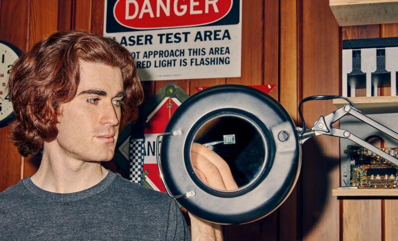
On eBay and other auction sites, he found inexpensive chip devices from the 1970s and 1980s that once belonged to California tech companies that later went out of business. Many pieces of equipment need to be repaired, but older machines are easier to repair than modern lab machines. One of The best discoveries Zelov thinks was a damaged electron microscope worth $250,000 in the early '90s; he bought it for $1,000 and fixed it. This electron microscope can check for defects in the chip.

Zelov repaired outdated equipment purchased online, including an electron microscope, to make his chips
Zelov sometimes had to improvise, like in a real chip factory, and he wanted to transfer the detailed design under the microscope to his equipment using a process called lithography. This requires coating the chip in a photosensitive material and burning it in the template using equipment such as an ultra-precision projector to guide subsequent processing steps. But the lithography machine was expensive, so Zelov installed a modified conference room projector on Amazon, which projected his designs on tiny scales onto silicon wafers, whose surfaces were covered with UV-sensitive materials.
In 2018, Zelov worked in his garage for about 12 hours to make the first chip, the Z1. In late 2018, Zelov began studying electrical engineering at Carnegie Mellon University and decided to upgrade the equipment in preparation for his second chip, the Z2. The Z2 uses a faster switching transistor design based on a wafer of a crystalline silicon called polysilicon that dominated in the 1970s.
Zelov's first chip, Z1, was manufactured in 2018 and has six transistors
Zelov hand-cuts the polysilicon half an inch square at 4,000 revolutions per minute on a small homemade turntable, each turning into a separate chip, transferring his design to the surface with photosensitive materials. He then implemented his design with a homemade lithography machine: a grid of 12 circuits, each with 100 transistors, for a total of 1200 transistors. Each chip is then etched with acid and heated in a furnace of about 1000 degrees Celsius, and phosphorus atoms are added to bake to adjust its conductivity. This is roughly similar to the way commercial fabs produce chips today, gradually adding and removing material from different parts of the design through a series of steps. The transistors on Zezelov's second-generation chips are about 10 times faster than the transistors on the first-generation chips, and their characteristics are as small as 10 microns, which is not much larger than red blood cells.
In August, Zelov connected the Z2 to a square beige semiconductor analyzer released by Hewlett-Packard about 20 years before he was born and tested it. On its glowing green screen, a series of smooth current-voltage curves mark its success. Zelov said: "It's amazing to see this curve, it's the first sign of life after you spent a whole day soaking this little crystal into a chemical beaker. ”
His second chip, Z2, was completed in August 2021 with 1200 transistors
Zelov said. His project garnered a lot of attention on Twitter, millions of views on YouTube, and some helpful tips from veterans of the semiconductor industry in the 1970s.
Zelov said he's not sure what he wants to do after graduation this spring, but he's been thinking about the place of DIY chip manufacturing in the modern tech ecosystem. Ellsworth's homemade transistors inspired Zelov, who believes chip technology, which is seen as obsolete, is still useful for engineers.
Zelov recently upgraded his lithography machine to about 0.3 microns or 300 nanometers of printed detail, roughly on par with the commercial chip industry in the mid-90s. "I want to push this design further and make people realize the possibility that we can do some of these kinds of things at home," he said.