TARGUS (Tigers) is a well-known notebook accessories in the United States old brand, used IBM, HP and other internationally renowned brands of laptop friends should have an impression of it, these brand notebooks attached to the bag mostly by TARGUS OEM. But today we will not talk about the TARGUS package, but disassemble its laptop adapter.
Recently, the charging head network got a laptop adapter from TARGUS, although the style is still traditional, but it supports 65W PD fast charging, which is very suitable for the current mainstream demand. The following charging head net will be disassembled in detail to see how the material works.
First, the appearance of the TARGUS 65W power adapter
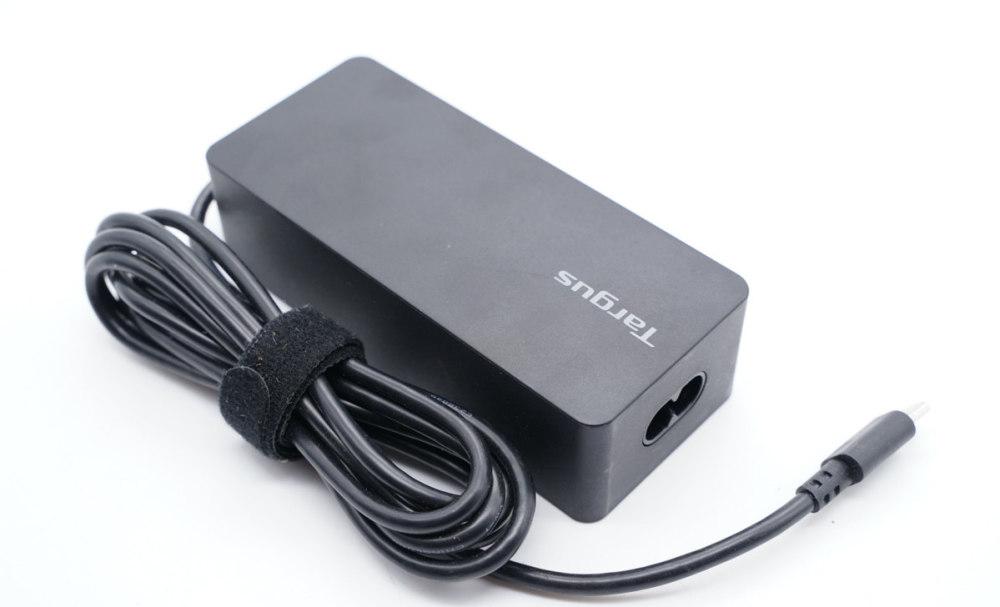
The adapter comes with its own USB-C output cable, the body is a classic box shape, the shell is frosted, and the top side is printed with the Targus logo.
The back of the fuselage is affixed with a parameter nameplate
Model: APA107
Input: 100-240V~50/60HZ 1.8A
Output: 5V3A, 9V3A, 12V3A, 15V3A, 20V3.25A, 3.3-21V3A
The adapter has passed CE, TUV certification, and also passed the VI energy efficiency certification.

The input is equipped with an 8-character socket.
The output cable is designed to be bend-resistant.
The thread head shell is frosted and designed with small concave surfaces for easy insertion and removal.
The measured length of the adapter body is 109.42mm.
The width is 47.62mm.
The thickness is 30.3mm.
The cable length is approximately 1.8 meters.
The total weight is about 229g.
The adapter measured using the Chargelab POWER-Z KT002 supports PD3.0 and PPS fast charging protocols.
In addition, it has five fixed voltage levels of 5V3A, 9V3A, 12V3A, 15V3A, 20V3.25A, and a set of PPS voltage gears of 3.3-21V3.25A.
Second, TARGUS 65W power adapter disassembly
The fuselage shell is cut open and the PCBA module wraps around the heatsink.
The measured module length was 85.25mm.
The width is 41.36mm.
The thickness is 24.67mm.
Remove the heat sink, the interior is a familiar scene, the side of the board is equipped with a heat sink, capacitors, transformers covered with a large amount of white glue.
The back of the board is the same, and the core components are all glued.
The white glue is cleaned up, and there is enough space around the transformer to effectively avoid heat accumulation.
At a glance on the back of the PCB board, there is a switching power supply PWM controller, a synchronous rectifier chip, a protocol chip, and an output VBUS switch.
At the input end, the high-voltage filter electrolytic capacitor is transverse, and there is a rectifier bridge fixed on the side heat sink.
Close-up of the delay fuse with a specification of 3.15A 250V.
Safety X capacitor close-up, capacity 0.47μF.
Common mode inductor flat copper strip wound for filtering out EMI interference.
Close-up of the GBP410 fairing bridge.
The high voltage filter electrolytic capacitor is from Chengxing and has a specification of 420V 120μF.
Close-up of the color ring inductance.
The main control chip power supply capacitor is also from Chengxing, with a specification of 100V 4.7μF.
PWM control close-up, silk screen 632L05.
The primary switching MOS tube adopts Fuding advanced AP60AN750, with a withstand voltage of 600V and a conductivity of 0.75Ω.
The other end is equipped with a transformer, Y capacitor, output filter capacitor.
Transformer close-up.
Y capacitance close-up.
Tongjia LD8926AA1 series secondary synchronous rectifier, synchronous rectifier MOS integrated controller, cost saving and board area, withstand voltage 100V, conduction resistance 12mΩ, support a variety of operating modes and protection functions.
Two output filter capacitors from Chengxing are 25V 680μF.
The protocol chip adopts Weiyi WT6636F, which is a protocol chip (TID number: 1080018) certified by the USB-IF Association USB PD3.0 (PPS), and has also passed the Qualcomm QC4+ certification, certification number QC20200316138.
WT6636F supports USB PD3.0 and PPS, built-in programmable constant voltage constant current control, integrated low-side current sampling amplifier, support for line loss compensation, support for multiple protection functions, including overvoltage protection of data pins, internal integration of 10bit ADC for voltage and current sensing, built-in 8051 core microcontroller, built-in discharge MOS tube.
Output VBUS switch tube close-up, Fuding AP4024EM, NMOS, withstand voltage 30V, conduction resistance 4.5mΩ.
All disassembled, let's take a family portrait.
Charging head net disassembly summary
TARGUS this adapter comes with a USB-C output cable, and the length is up to 1.8 meters, plus the power cord, the overall length can meet the needs of many daily scenes. In addition, in addition to having a complete fixed voltage gear of 5-20V, this adapter also supports PPS fast charging, with a set of 3.3-21V3.25A PPS voltage gears, which is still relatively rare.
Through disassembly, the charging head network found that this adapter adopts the classic QR switching power supply architecture, and the secondary side adopts a synchronous rectification chip LD8926AA1 with integrated MOS for rectification output, and the WT6636F protocol IC controls the output voltage. The input and output filters are carried out by Chengxing capacitors, and the internal design and workmanship conform to the consistent style of the laptop adapter.