Zhi Dongxi (public number: zhidxcom) wen | lina
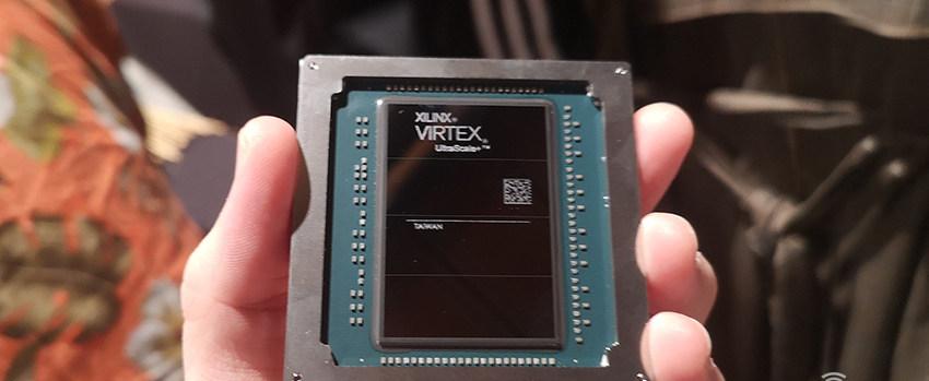
On August 21, Silicon Valley reported that Xilinx's first innovation day is being held in Silicon Valley. On the night before the innovation day, Xilinx officially launched the largest fpga chip "ever" - virtex ultrascale + vu19p, and Zhidong also saw the actual product of this chip for the first time on the spot, and learned more performance and parameter information.

Xilinx's vu19p chip is not only huge in size and capacity, but also has greater industrial significance than the world's largest giant chip produced by the American startup Cerebras a few days ago.
vu19p uses 16nm process, based on arm architecture, has 35 billion transistors, and also has the highest logic density and maximum number of i/o (9 million system logic units and 2072 user i/o interfaces) of a single chip ever recorded for simulation and prototyping of the most advanced AI chips, 5G chips, and automotive chips, which will be available in the fall of 2020.
At the ongoing Xilinx Innovation Day, Xilinx cto and senior vice president ivo bolsens, vice president ken chang, senior director of the Office of the Chief Technology Officer patrick lysaght and other technology leaders will further interpret Xilinx acap architecture, the future development direction of data processing and extension system architecture, transistor/packaging/interconnection development and other topics. Zhi Dong will also send back at the scene for the first time.
Hanneke Krekels, Senior Marketing Director of Xilinx Test measurement simulation, and Mike Thompson, Senior Product Line Manager, Xilinx Virtex Ultrascale+ Series
Mike Thompson, senior product line manager at Xilinx ultrascale+ series, said that vu19p was born for all the most cutting-edge chips on the market today that need to be simulated and prototyped with fpga chips before tape-out, and it is a "chip maker's chip" (chip for chipmakers)
vu19p can also support a variety of complex emerging algorithms, such as artificial intelligence, machine learning, video processing, sensor fusion, and so on. Sumit Shah, senior director of marketing and management for Xilinx's product line, said VU19p not only helps developers accelerate hardware validation, but also helps them integrate software before asc or soc is available.
In addition to hardware technology, Xilinx offers vivado design kits and toolflows and IP support for users, allowing chipmakers to integrate software before chips are available, reducing costs, mitigating tape-out risk, increasing efficiency, and accelerating time to market.
In terms of specific parameters, the vu19p integrates 16 arm cortex-a9 CPUs, has 9 million system logic units, 1.5 terabits per second of ddr4 memory bandwidth, 4.5 terabits per second of transceiver bandwidth, and 2072 user i/o interfaces.
According to Xilinx, Xilinx is the holder of the global record for the "largest capacity" FPGA of three generations – the first is the 2011 elite-7 2000t, the second is the 2015 virtex ultrascale vu440, and the third generation is the now 2019 virtex ultrascale+ vu19p.
Compared to the previous generation of "champions" - 20nm ultrascale 440 fpgas - the new generation of vu19p increases capacity by 1.6 times, while also reducing system energy consumption by 60%.
The number and bandwidth of vu19p's I/O interfaces are also 1.4 times that of the previous generation, which is convenient for users to achieve scalability, debugging and practical verification.
At the same time, vu19p also has 80 28g transceivers, which can be applied to high-port density measurement devices, supporting the latest interface standard verification system design and verification.
Now all the most cutting-edge chips on the market need to be simulated and prototyping with fpga chips before tape-out, so this vu19p launched by Xilinx is for chip manufacturers, which can support more complex AI, 5G, automotive, vision algorithms, and can also support larger-scale ASIC/SOC design needs.
As the current chip manufacturing process becomes more and more sophisticated, chip design becomes more and more complex, the upfront cost of chip designers soars, and the risk of tape-out is further improved, and the demand for reducing chip costs/reducing tape-out risk/shortening time to market will further explode.