Jiwei Network reported that test equipment is mainly used to detect chip performance and defects in the semiconductor manufacturing process, and almost every step of the main process needs to be carried out after completion, running through the beginning and end of the entire semiconductor production.
In the face of the rapidly advancing semiconductor process technology, how can the semiconductor test equipment with the ultra-long "standby" service always walk in front of the measured chip? With the continuous upgrading of semiconductor processes and the increasing complexity of downstream applications, the role of testing, which is inseparable from the semiconductor industry, is also constantly enriching and deepening.
"Carrying on from top to bottom": The deepening role of testing
According to the focus of the test needs of different types of chips, the main segments of semiconductor test machines are memory, SoC, analog, digital, discrete devices and RF test machines. Globally, the ATE market is dominated by memory and SoC testing. There is still a good market space in China in the fields of simulation testing and discrete device testing. Among them, the SoC test machine is mainly for the SoC chip (System on Chip), that is, the test system of the system-on-chip design; the storage test machine is mainly tested for memory, generally by writing some data after reading back and verifying for testing. Among them, the SoC and storage test machine are the most difficult, and at the same time, the structural proportion is also the largest part of the test machine, accounting for about 70% in the global and domestic markets. For example, the 2020 annual report of the global ATE head manufacturer Edwin Test disclosed that it achieved revenue of $2.552 billion in fiscal 2020, and the SoC chip testing and memory chip testing business accounted for 81% of the company's total revenue, of which SoC chip testing accounted for 57%, memory chip testing accounted for 24%, and its sales in the Chinese mainland and Taiwan markets exceeded 60%.
Semiconductor test machines usually have to be "ultra-long" standby to serve the industry, and the time span is often calculated in the dimension of 10 years. In the past few decades, from a technical point of view, the semiconductor test industry has not been greatly innovated for a long time. But now with the rise of emerging markets such as 5G, big data, artificial intelligence, and autonomous driving, the semiconductor industry is being driven by many drivers to enter a stage of rapid development. Chips have entered the era of integration, the direct change is that there are more and more functions on a chip, and the chip process is becoming more and more complex, which not only means that the complexity of the test will also increase exponentially, but also makes the yield of the chip more dependent on the advanced functions of the test.
"The role of traditional test manufacturers is to tell you whether a chip is good or not, but this single role is obviously far from meeting the needs of the moment." Ge Liang, senior manager of business development of EdWan Test (China), pointed out to Jiwei Network a few days ago, "Now the test equipment needs to provide not only whether the chip is good or not, but also to provide how good it is, how bad it is, where the problem is, and how to improve it." ”
The role of testing across the value chain is changing as technology advances in the industry. In fact, with the improvement of the complexity of chip technology, testing has an increasingly important role in the entire industrial chain, and the role is constantly enriched and deepened. "From the point of view of testing, it is also necessary to expand to the left and right of the industrial chain, to the right can help the application of the system level in the back, and to the left can also help the production process and design in the front." Ge Liang explains.
It is worth noting that "Shift Left" is a concept that has been constantly discussed by the entire semiconductor industry in recent years. The term originated in the software industry and refers to finding and fixing bugs early in the development process, rather than rediscovering them during post-release testing, as it costs 100 times more to fix them after release. This cost in the semiconductor industry is obviously higher. Specific to semiconductor testing, this concept is also needed.
Specifically, facing the application side on the right, after the chip is made, it is to be installed in the system to be used, and it is necessary to further test whether the performance in the system is good. And sometimes, a chip or system is just measured out is good, but there may be some potential factors that lead to its reliability in the back is not very high, through the test to further provide its service life, reliability, etc., these are also to be screened out through the test, especially in the field of vehicle chips, reliability is the most critical factor.
Facing the left side of the industrial chain, the test should be feedback, is the part of the IC design good enough? Does the IC design provide sufficient test access? Is there a process problem at the production end? How the back section of the industrial chain helps the design, production process, packaging process, etc. of the front section is also a part that the current industry attaches great importance to.
The more high-end and complex chips are, the more dependent they are on testing, and the advanced capabilities of test devices are becoming increasingly important for semiconductor vendors such as 5G, IoT, and cloud computing. The role of semiconductor test equipment manufacturers (ATEs) has also evolved with the development of the industry. At present, in the global ATE market pattern, Teradyne and EdWin have formed a comprehensive product series such as SoC testing, memory testing, analog signal testing, digital-analog mixed-signal testing, etc., and have actively developed and laid out emerging trends such as 5G, AI, and the Internet of Things, representing the level of the industry's forefront.
In the case of EdWin Test, for example, EDM Test has been deepening its role as its most tested manufacturer for more than six decades – from initial chip-level testing to system-level testing to end-to-end testing, EdWin Testing has been "pursuing customer value in the evolving semiconductor value chain." ”
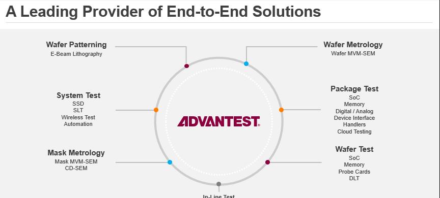
At present, Edwin's tested products have fully covered from wafer lithography testing to system-level testing and then to end-to-end testing, covering almost all tests including memory, SoCs, LCD chips, MCUs and sensor ICs.
Testing is always ahead of the chip
For test manufacturers, it is not to catch up with market trends, but to predict the next generation of trends. Because the test instrument must go ahead of the chip being tested.
And how to make the test machine with a long standby cycle always go ahead? That means that high-end test machines must evolve towards scalability test platforms, with flexibility, compatibility, and scalability being key capabilities. On a single platform, through the evolution and expansion of hardware boards and software tools, its testing capabilities and application scope are continuously improved to face new requirements and maximize the protection of users' investment in equipment and technical capabilities.
For example, the V93000 test machine tested by Edwin was first launched in 1999. For more than 20 years, it has maintained stable sales and shipments. But it is no longer the test machine of more than 20 years ago, and it has undergone four generations of Upgrades of Single Density, Pin Scale, Smart Scale, and EXA Scale to meet the evolving testing needs while still maintaining its user interface approach to hardware and software.
"We usually look forward 5 years, and the cross-generation cycle of chip technology development is generally 5 years. So you have to know, what kind of capabilities are needed for chips after 5 years? What needs to be tested? Ge Liang stressed that in order to be accurate, it is necessary to communicate and cooperate closely with enterprises in the industrial chain, "Many research and development ideas and programs are actually generated by mutual stimulation with industrial chain customers." ”
Jiwei Network learned that when Edwin tests and formulates new product directions and strategies, it usually adopts a "combination of general and specialized" methods, that is, a combination of general solutions and special solutions. Taking memory chips as an example, most of the memory chips are general-purpose chips, usually the company will repeat communication with several major memory manufacturers around the world before releasing the next generation of memory test products, understand their needs, in order to ensure the publicity of the next generation of products, which is the "pass" part; but also consider the unique needs of each customer and the test cost of each family, to do some customized solutions. However, there is sometimes a transformation between the pass and the special. When several leading manufacturers adopted a certain scheme at an early stage, and then it is likely that the entire market will follow this model, then some dedicated customized solutions may slowly be transformed into general solutions accepted by the market.
Collaborative development and launch of solutions has gradually become the mainstream direction of cooperation between test vendors and the industrial chain. Semiconductor test machine needs to support the test requirements of chips, joint development with IC design manufacturers, based on long-term development cooperation, test machine manufacturers can also further accumulate a large number of patents and R & D experience, and cooperate with design companies to form tacit cooperation and gradually establish an ecology.

Therefore, the test machine manufacturers that bind IC design manufacturers in the early stage for joint development often have a greater probability of obtaining orders, and once they enter the design company cooperation system, they will have significant customer resource barriers and industrial collaboration barriers.
In the post-Moore era, the importance of "test first" was prominent
But in fact, for IC vendors, it is also becoming more and more critical to bind joint development test solutions with test vendors at an early age. In the past, most people may think that chip testing is that customers can talk to test manufacturers about test plans after designing products, but now the situation is more likely, when they have a basic idea prototype, it is best to start in-depth communication with test manufacturers, so as to ensure that their products can be designed or designed in the process, you can establish the corresponding test program, you can gradually verify.
The value of testing is mainly reflected in the two aspects of time-to-market and yield improvement. The inspection equipment itself does not change the texture of the wafer or chip, but the optimized test method can control costs and reduce theDPPM (Defective Parts Per Million) in the end customer with high test coverage, reducing the return rate.
As the industry enters the era of chip integration, the complexity of processes and applications continues to increase, and if the semiconductor industry wants to make good products, it needs to pay more attention to "test first". Especially in the post-Moore era, in the case that the process process cannot be further improved, advanced packaging has become a major direction of attention in the industry, 2.5D packaging, 3D packaging, SiP, etc. This has put forward higher requirements for wafer-level testing, which further highlights the importance of testing first.
Because, traditionally, a chip is usually measured relatively simply at the wafer-level test level, and will be tested more completely after the package is completed. But now, due to the greatly increased complexity of advanced packaging, it may involve a bunch of chips including storage, CPU, GPU, etc., and they are all expensive, but if there is a bad chip, it may drag down all other chips. Therefore, in the era of advanced packaging, many tests need to be advanced, such as the original system-level tests in the back may be done in advance to the wafer level to ensure the overall yield.
At the same time, with the integration of technology, the boundaries between the value chains of the semiconductor industry tend to blur. Test manufacturers and semiconductor customers tend to be in a "you have me, I have you" state, and it is necessary to cooperate in the development of test solutions at a very early stage, including the design of the entire test process, the adjustment of machine equipment and so on.
Undoubtedly, whether from the perspective of product technology or market layout, the development process of semiconductor testing is closely related to the global semiconductor industry. Chip technology is becoming more and more complex, which also means that there is still more room for growth and development of test technology.