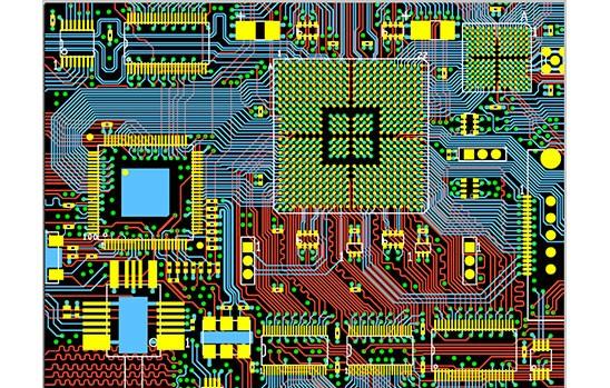
Shenzhen Lingzhuo Electronics is a professional PCB design company with an average of more than 20 years of work experience in PCB design team, which can provide multi-layer, high-density, high-speed PCB wiring design and PCB design proofing services. Next, I will share with you how PCB design distinguishes between analog and digital.

Why distinguish between analog and digital in PCB design?
In simple terms, digitally is the common reference terminal of the digital circuit part, that is, the reference terminal of the digital voltage signal; Analog ground is the common reference of the analog circuit section, and the voltage reference of the analog signal (zero potential point).
Since digital signals are generally rectangular waves, they carry a large number of harmonics. If the digital ground in the board is not separated from the analog ground from the access point, the harmonics in the digital signal can easily interfere with the waveform of the analog signal. When the analog signal is a high-frequency or strong electrical signal, it will also affect the normal operation of the digital circuit. Analog circuits involve weak signals, but the higher threshold levels of digital circuits make the power supply less demanding than analog circuits. In a system with both digital circuits and analog circuits, the noise generated by the digital circuit will affect the analog circuit, making the small signal index of the analog circuit worse, and the way to overcome it is to separate the analog and digital.
The root cause of the problem is that the resistance of the copper foil on the circuit board cannot be guaranteed to be zero, and the separation of digital ground and analog ground at the access point is to minimize the common ground resistance of digital ground and analog ground.
What are the design methods in PCB design that distinguish between analog and digital?
There are generally several methods for dealing with analog and digital land:
Ø Directly separated, in the schematic, the ground of the digital area is connected to DGND, the ground of the analog area is connected to AGND, and then the ground plane in the PCB is divided into digital ground and analog ground, and the spacing is widened;
Ø Digital ground and analog ground are connected with magnetic beads;
Ø The digital ground and the analog ground are connected with capacitors, and the principle of capacitive isolation straight-through cross is used;
Ø The inductive connection between digital ground and analog ground, the inductance value varies from uH to tens of uH;
Ø The digital ground and the analog ground are connected with zero ohm resistance.
In summary, the capacitor barrier is straight through the cross, causing floating ground. The capacitor is not direct current, which will lead to the accumulation of differential pressure and static electricity, and the touch case will be numb. If the capacitor and the magnetic bead are connected in parallel, it is a snake to add to the snake, because the magnetic bead is straight, and the capacitor will fail. In tandem, it seems to be incomparable.
The inductor is large in size, there are many stray parameters, the characteristics are unstable, the discrete distribution parameters are not easy to control, and the volume is large. The inductor is also a notch, and the LC resonance (distributed capacitance) has a special effect on noise.
The equivalent circuit of the bead is equivalent to a band trap, only for a certain frequency point of the noise has a suppressive effect, if you can not predict the noise, how to choose the model, moreover, the noise frequency is not necessarily fixed, so the bead is not a good choice.
The 0 ohm resistor is equivalent to a very narrow current path, which effectively limits the loop current and suppresses the noise. Resistors have attenuation in all frequency bands (0 ohm resistance also has an impedance), which is stronger than beads.
In short, the key is to be grounded a little bit in analog and digital. It is recommended that different kinds be connected with 0 ohm resistors; Beads for the introduction of high-frequency devices into power supplies; Small capacitance for coupling of high-frequency signal lines; Inductors are used on high-power low frequencies.
The above is how PCB design distinguishes between analog and digital introduction, I hope to help everyone, and if you want to know more about PCB design information, you can pay attention to the update of Lingzhuo proofing.