The layered compound AVSb (A = K, Rb, and Cs) with vanadium Kagome lattice contains a wealth of physical phenomena such as topological non-mediocre electron structures, superconductivity, and charge density wave (CDW) transitions, which have attracted widespread attention from researchers.
At atmospheric pressure, AVSb undergoes a CDW transition (q=2a×2a and q=4a) at 78-103 K, causing a time-inversion symmetry breakdown, which may be one of the causes of the large anomalous Hall effect; the superconducting critical temperature (Tc) of the bulk sample is 0.93-2.5 K. Through high-voltage in situ studies, the researchers found that CsVSb was in the low-pressure region (0-2 GPa), CDW was gradually suppressed, and Tc had a non-monotonic "M" phase diagram and gradually disappeared [Nature Commun. 12, 3645 (2021); Phys. Rev. Lett. 126, 247001 (2021)]。 But when the pressure rises to 15 GPa, CsVSb undergoes superconductivity re-entry, and superconductivity stabilizes to 100 GPa [Highly Robust Reentrant Superconductivity in CsVSb under Pressure, Chin. Phys. Lett. Express Letter 38, 057402 (2021)]。
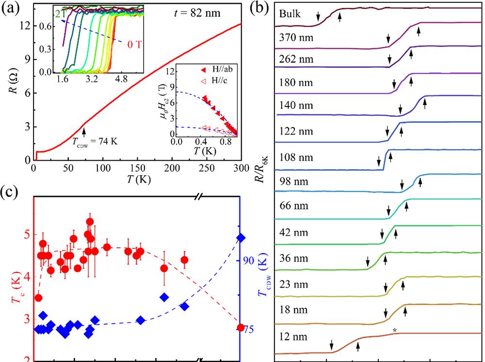
Figure 1: Low temperature transport characteristics of a thin layer sample of CsV3Sb5
From the perspective of energy band structure, the Fermi level of CsVSb is located near the two VanKhov singular points (VHS), and the position and state density of the Fermi energy level can be adjusted through charge doping, effectively increasing the Tc of CsVSb.
Recently, Yanpeng Song, Tianping Ying, Guo Jiangang and Xiaolong Chen, postdoctoral fellows from the Advanced Materials and Structure Analysis Laboratory of the Institute of Physics of the Chinese Academy of Sciences/Beijing National Research Center for Condensed Matter Physics, in collaboration with Dr. Wu Xianxin and Professor Andreas P. Schnyder of the Max Planck Institute for Solids in Germany, have achieved the first effective regulation of cavitation carrier doping and TC in CsVSb. Due to the weak interlayer force of CsVSb, the project team obtained CsVSb samples of different thicknesses (12-370 nm) by mechanical stripping, and achieved hole doping at different concentrations by controlling the oxidation degree of Cs atoms, and obtained a dome-like superconducting phase map of Tc changing with the amount of doping. Among them, the highest Tc is 5 K, and CDW and superconductivity show a competitive relationship, see Figure 1.
At the same time, the project team carried out in-situ gate pressure regulation on the thin layer sample of CsVSb, and found that its Tc decreased with the increase of positive gate pressure, which proved that the sample did indeed belong to the hole type doping, which was also the first in situ gate pressure regulation experiment on CsVSb. Density functional theory calculations show that one of the two VanKhov odd points near the Fermi surface (VHS1) and the density of the state are extremely sensitive to changes in cavity doping, qualitatively explaining the change in Tc, see Figure 2.
This work provides a new regulatory pathway for studying and understanding the interrelationships between superconductivity, CDW and topology in AVSb, published in Physiological Review Letters [Phys. Rev. Lett. 127, 237001 (2021)]。

Figure 2: Band structure, state density (DOS), and phase diagram of hole-doped CsVSb
The above work has been supported by the Chinese Academy of Sciences, the National Key Research and Development Program, the National Natural Science Foundation of China and the Beijing Municipal Natural Science Foundation.
Edit: Fun Superman